Vertical stacking of multiple integrated circuits including SOI-based optical components

An integrated circuit, vertical stacking technology, applied in the direction of optical waveguide, light guide, etc., can solve problems such as wafer bending

Inactive Publication Date: 2008-02-20
SIOPTICAL INC
View PDF0 Cites 7 Cited by
  • Summary
  • Abstract
  • Description
  • Claims
  • Application Information

AI Technical Summary

Problems solved by technology

However, buried oxides with a thickness of 1 micron lead to significant bowing of the wafer, especially when compared to the planarity requirements of very fine line widths of advanced electronic devices

Method used


Image

  • Vertical stacking of multiple integrated circuits including SOI-based optical components
  • Vertical stacking of multiple integrated circuits including SOI-based optical components
  • Vertical stacking of multiple integrated circuits including SOI-based optical components

Examples


Embodiment Construction

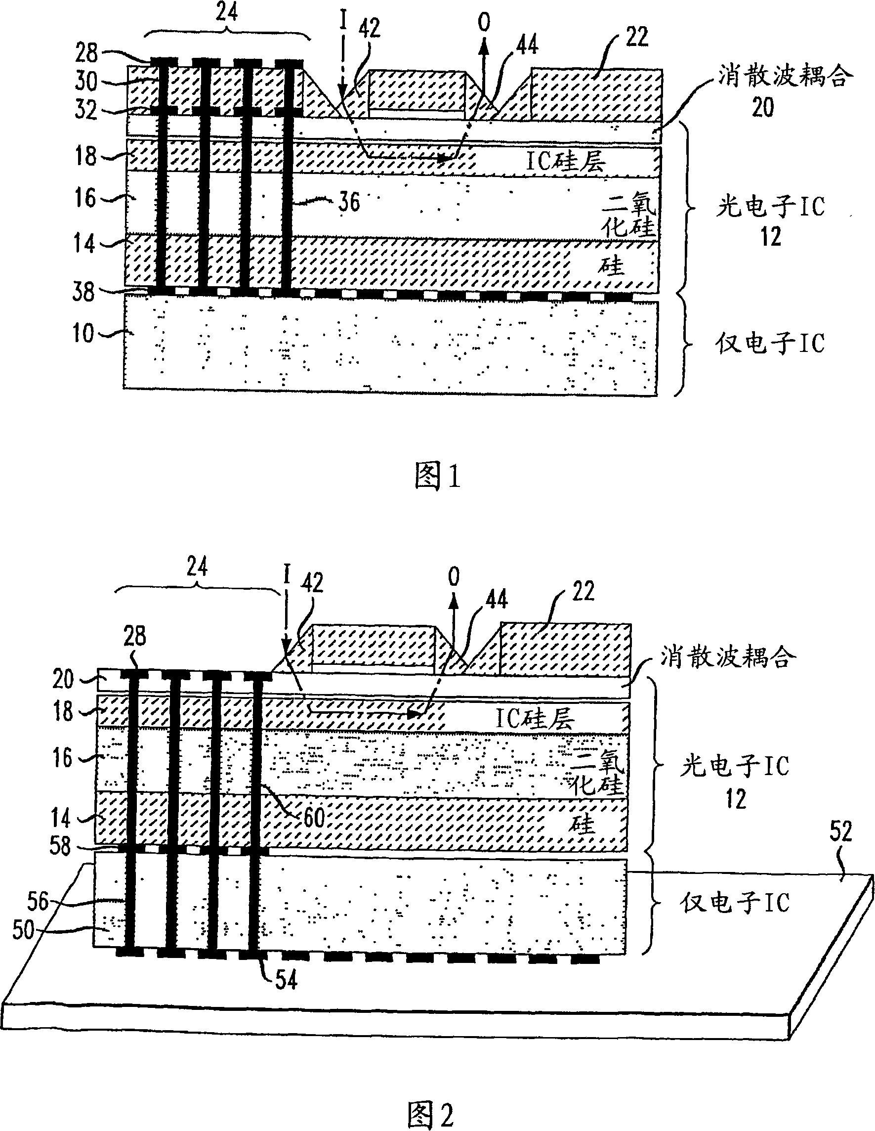
[0019] Figure 1 shows in cutaway side view a typical vertically stacked device formed in accordance with the present invention. As shown, the device includes a first integrated circuit (IC) 10 comprising electronic circuitry, wherein the IC 10 is fabricated using conventional CMOS processing techniques. In practice, fine linewidth lithography as described above can be used to form elements in IC 10 . An SOI-based optoelectronic circuit 12 is arranged above the electronic IC 10 in the manner shown in FIG. 1 . As is well known in the art, SOI-based circuitry 12 includes a base silicon substrate 14, a buried oxide layer 16, and a relatively thin silicon surface layer 18 (hereinafter "SOI layer"). Although not specifically illustrated in FIG. 1 for clarity, this layer may include differently doped regions and / or other sub-layers (e.g., polysilicon, interlevel dielectric, and metallization) needed to form the desired passive and active optical devices. ). For this particular emb...


PUM


Abstract

A vertical stack of integrated circuits includes at least one CMOS electronic integrated circuit (IC), an SOI-based opto-electronic integrated circuit structure, and an optical input/output coupling element. A plurality of metalized vias may be formed through the thickness of the stack so that electrical connections can be made between each integrated circuit. Various types of optical input/output coupling can be used, such as prism coupling, gratings, inverse tapers, and the like. By separating the optical and electrical functions onto separate ICs, the functionalities of each may be modified without requiring a re-design of the remaining system. By virtue of using SOI-based opto-electronics with the CMOS electronic ICs, a portion of the SOI structure may be exposed to provide access to the waveguiding SOI layer for optical coupling purposes.

Description

[0001] Cross References to Related Applications [0002] This application claims the benefit of US Provisional Application No. 60 / 650,061, filed February 4, 2005. technical field [0003] The present invention relates to vertical stack packaging of multiple integrated circuit chips, and more particularly to vertical stacking for SOI-based optical components and associated electronic integrated circuits. Background technique [0004] The standard CMOS lithographic design rules for today's electronic integrated circuits (ICs) use 90nm linewidths, very likely down to 65nm and below, perhaps down to fine linewidths of about 22-32nm (or less). While this thinner linewidth lithography is acceptable for electronic applications, it poses problems for silicon-on-insulator (SOI) applications that attempt to incorporate optical devices into electronic devices within the same structure. In particular, the buried oxide in SOI structures must be approximately 1 micron in thickness for op...

Claims


Application Information

Patent Timeline
Patent Type & Authority Applications(China)
IPC IPC(8): G02B6/12
Inventor 卡尔潘都·夏斯特里威普库马·帕特尔戴夫·佩德约翰·芳曼
Owner SIOPTICAL INC
Why Eureka
Try Eureka