Radiating type thin-film flip-chip packaging construction

A thin-film chip-on-chip packaging and heat-dissipating technology, which is applied in the direction of electrical components, electrical solid devices, circuits, etc., can solve the problems of inconvenience, general products without structure, etc., and achieve the effect of improving adhesion

Inactive Publication Date: 2008-02-27
CHIPMOS TECH INC
View PDF0 Cites 2 Cited by
  • Summary
  • Abstract
  • Description
  • Claims
  • Application Information

AI Technical Summary

Problems solved by technology

[0009] It can be seen that the above-mentioned existing film-on-chip package structure obviously still has inconvenience and defects in structure and use, and needs to be further improved urgently.
In order to solve the above-mentioned problems, the relevant manufacturers have tried their best to find a solution, but no suitable design has been developed for a long time, and the general products do not have a suitable structure to solve the above-mentioned problems. This is obviously related. The problem that the industry is eager to solve

Method used


Image

  • Radiating type thin-film flip-chip packaging construction
  • Radiating type thin-film flip-chip packaging construction
  • Radiating type thin-film flip-chip packaging construction

Examples


no. 1 Embodiment

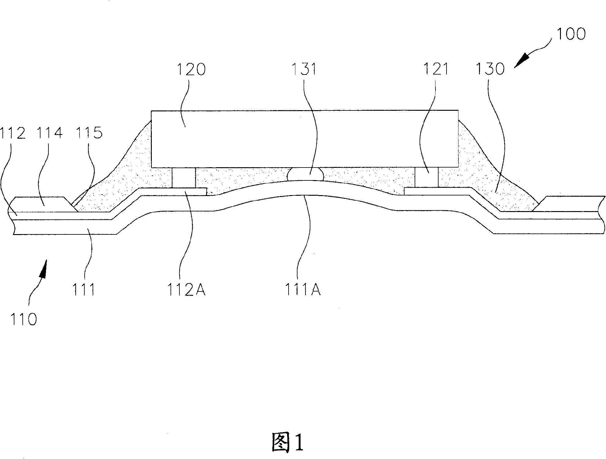
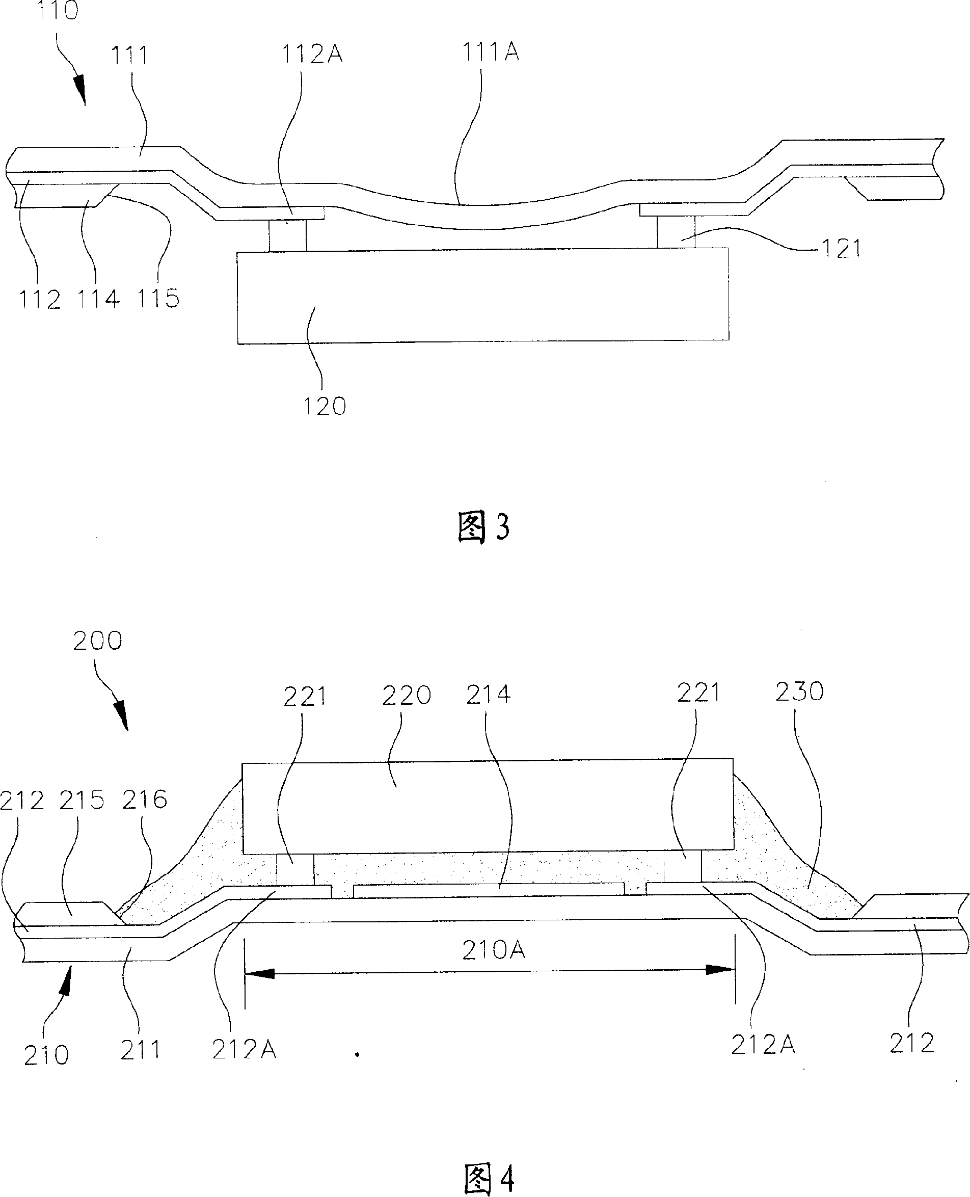
[0059] Please refer to FIG. 4 , which is a schematic cross-sectional view of a chip-on-film packaging structure according to the first preferred embodiment of the present invention. According to the first embodiment of the present invention, a chip-on-film package structure is disclosed. The chip-on-film package structure 200 mainly includes a circuit film 210 , a chip 220 and a dot-coated glue 230 . The chip 220 is bonded to the circuit film 210, and the circuit film 210 defines a flip-chip bonding area 210A corresponding to the chip 220 and having a roughly rectangular shape (as shown in FIG. 5 ).

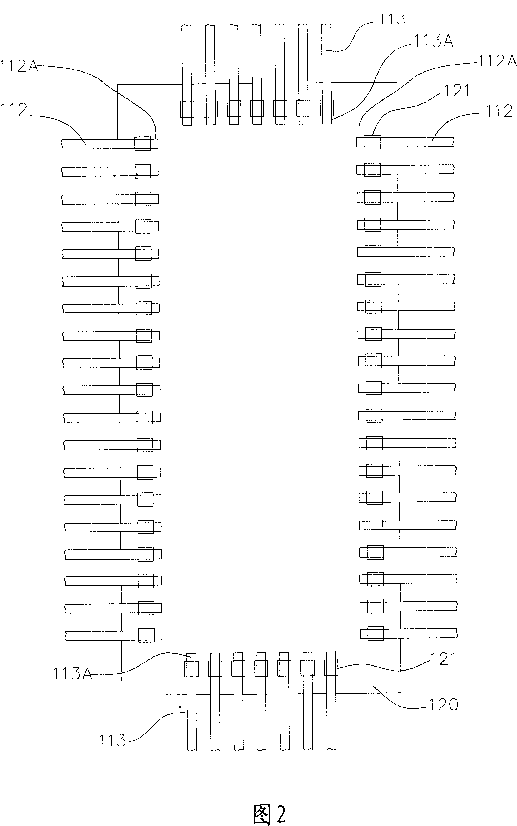
[0060] Please refer to FIG. 4 and FIG. 5 . FIG. 5 is a bottom perspective view of a chip-on-film packaging structure according to a first preferred embodiment of the present invention. The above-mentioned circuit film 210 has a soft dielectric layer 211 , a plurality of long side leads 212 , a plurality of short side leads 213 and a supporting copper pad 214 . Usually, the mater...


PUM


Abstract

The present invention relates to a heat-dissipated-and-Chip-On-Film package, and mainly includes a circuit film, a protruded wafer and a point-coated colloid. The circuit film is defined with a pair of joint regions of wafer which correspond to the wafer, and has a soft dielectric layer, even numbers of pins and a supporting copper pad. Even numbers of inner joints of the pins are arranged around the joint regions of wafer, and the supporting copper pad is formed in central of the joint regions of wafer, thus collapse of the soft dielectric layer during combination of the protrusions of the wafer and the inner joints of the pins can be avoided. Therefore, the point-coated colloid can be successfully filled between the circuit film and the wafer, and no bubble will occur.

Description

technical field [0001] The present invention relates to an integrated circuit packaging structure, in particular to a method that can prevent the soft dielectric layer from collapsing when the bumps of the chip are bonded to the inner joints of the pins, so that the dispensing glue can be smoothly filled on the circuit film Between the chip and the chip, there will be no air bubbles in the heat-dissipating type film-on-chip packaging structure (Chip-On-Film package). Background technique [0002] In the past integrated circuit packaging structure, a chip-on-film packaging structure is designed for a long rectangular display driver chip, which is respectively provided with a gold bump on the input end and output end of the two long sides of the chip, and through Compression and heat are applied to bond to leads of a circuit film. When the heating temperature of the wafer is transferred to the circuit film, it often causes the circuit film to collapse when heated, resulting i...

Claims


Application Information

Patent Timeline
Patent Type & Authority Applications(China)
IPC IPC(8): H01L23/498H01L23/12H01L23/28H01L23/36
CPCH01L2224/73204
Inventor 杨郁廷
Owner CHIPMOS TECH INC
Why Eureka
Try Eureka