SiSb based phase-change thin-film material used for phase-change memory device

A phase-change memory and thin-film material technology, which is applied in the field of materials in the field of microelectronics technology, can solve problems affecting the contact between phase-change thin films and electrodes or other film layers, affecting device stability, and unfavorable device operation, etc., to achieve superior amorphous State stability, fast crystallization rate, and good compatibility

Inactive Publication Date: 2008-02-27
SHANGHAI JIAO TONG UNIV +1
View PDF1 Cites 3 Cited by
  • Summary
  • Abstract
  • Description
  • Claims
  • Application Information

AI Technical Summary

Problems solved by technology

In this process, the thickness of the phase change film will change, if the change is too large, it will affect the contact between the phase change film and electrodes or other film layers, thus affecting the stability of the device
Common Ge 2 Sb 2 Te 5 The thickness of the film in the amorphous state and the crystalline state varies greatly (6.8%), which is not conducive to the long-term stable operation of the device

Method used


Image

  • SiSb based phase-change thin-film material used for phase-change memory device

Examples


Embodiment 1

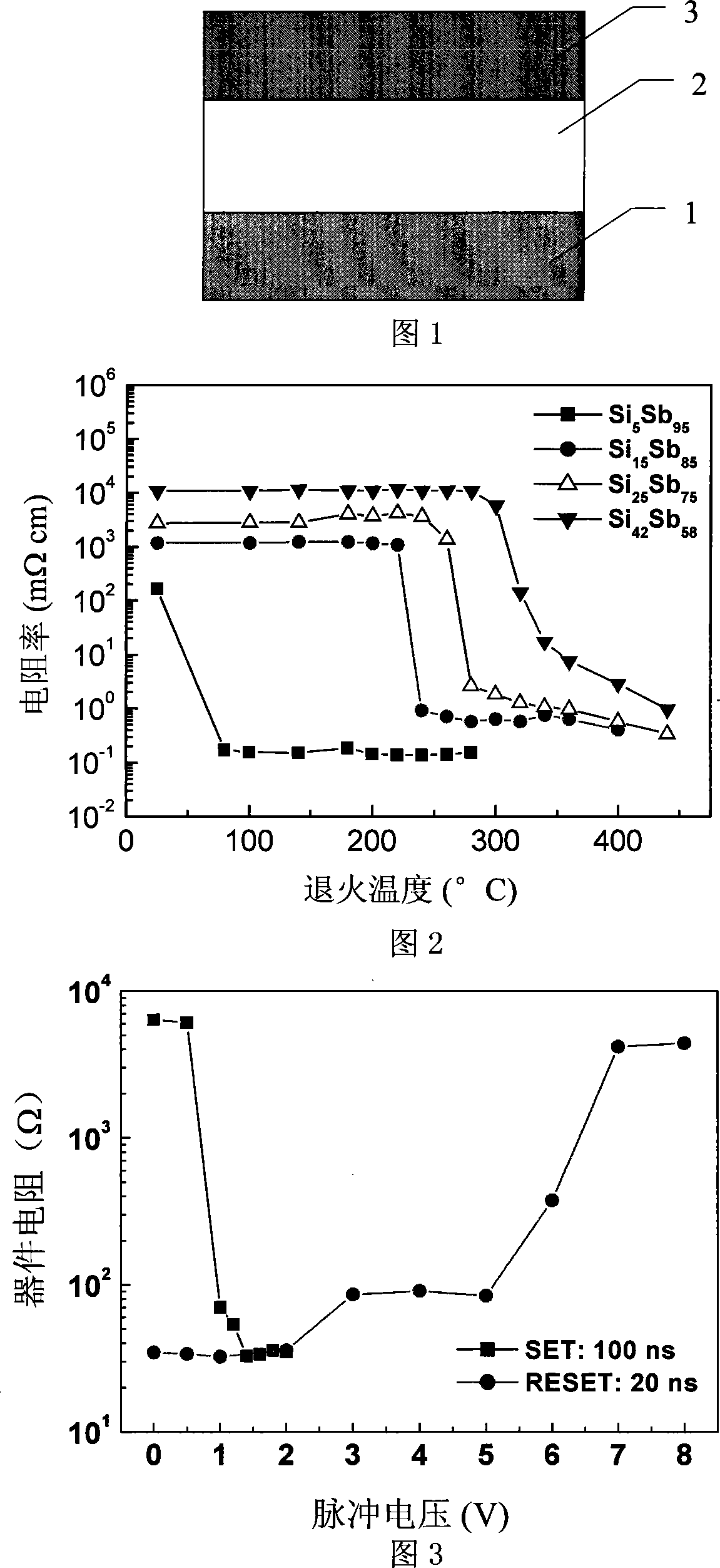
[0022] The phase change material series is a SiSb-based phase change film, that is, when the doping element content y is 0, the specific composition is Si x Sb 1-x , wherein the Si content x is 5-90% atomic percent. A particularly suitable composition is that the Si content can be 10-60 atomic percent.

[0023] Figure 2 shows Si with different Si content x Sb 1-xThe relationship between film resistivity and annealing temperature. When the film is in an amorphous state, the film resistance is in a high resistance state, and as the annealing temperature increases, the film begins to crystallize, and when the film crystallizes, the film resistance is in a low resistance state. This process is realized in the memory device by heating the phase-change film with electric pulses, and the reversible transition between the high-resistance state and the low-resistance state can be achieved by applying different electric pulses. When Si content x is 5%, Si 5 Sb 95 The crystallizat...

Embodiment 2

[0035] The phase change material series is doped Si x Sb 1-x Alloy film: (Si x Sb 1-x ) 1-y m y , wherein the doping element M can be 0 element or N element or their mixture, the content y of the doping element M is 0-15 atomic percent, and the Si content x is maintained at 5-90 atomic percent.

[0036] In a specific embodiment, an oxygen-doped SiSb-based phase change film is prepared by reactive sputtering. Oxygen doping can also be implemented by implanting oxygen ions into the SiSb phase change film. Oxygen-doped Si x Sb 1-x The relationship between resistivity and annealing temperature of the phase change film is similar to that in Figure 2, that is, as the annealing temperature increases, the film crystallizes and changes from a high-resistance state to a low-resistance state. Oxygen-doped Si x Sb 1-x Phase change films can also be used in phase change storage media. Oxygen doping makes Si x Sb 1-x The amorphous resistivity of phase change films can be increa...


PUM


Abstract

This invention relates to SiSb-based phase-transformation film material use for phase transformation storage cell. The components are: (SixSb1-x)1-yMy; wherein M=O element or N element or the mixture of both, the content of doping element M being y (atomic percentage)=0-15%, and the content of Si being x (atomic percentage)=5-90%. Reversible transition occurs between low resistance and high resistance when being subjected to electric pulse, so achieving the goal of data storage. This invention has advantages of: no use of toxic element Te, its production art can be compatibility with prior art semiconductor integrated circuit CMOS process. The inventive film has faster crystallization rate than commonly used Ge2Sb2Te5 film, excellent non-crystal stability, lower thickness transition rate of non-crystal / crystal film, so ircreasing storage speed, and also data reliability and device stability.

Description

technical field [0001] The invention relates to a material in the technical field of microelectronics, in particular to a SiSb-based phase-change thin film material used in a phase-change memory. Background technique [0002] The basic principle of phase change memory technology is to use phase change thin film material as storage medium. The resistivity of phase change thin film is very different between amorphous state and crystalline state. Using programmed electric pulse can make phase change thin film in amorphous state The reversible conversion between the crystal state and the crystalline state, so that the phase change memory cell can reversibly change between high resistance and low resistance. Moreover, the state of the storage unit is non-volatile, that is, when it is set to any state, even if the power is cut off, the storage unit still maintains the resistance value of the state, unless the state of the storage unit is reset. The memory cells are defined by por...

Claims


Application Information

Patent Timeline
Patent Type & Authority Applications(China)
IPC IPC(8): H01L45/00G11C11/56C22C12/00G11B7/243G11B7/2433G11B7/2437
Inventor 冯洁张胤蔡炳初陈邦明
Owner SHANGHAI JIAO TONG UNIV
Why Eureka
Try Eureka