TFT LCD panel electrostatic discharge protection circuit
An electrostatic discharge protection and circuit technology, which is applied to circuits, electrical components, and electrical solid devices, etc., can solve problems such as static discharges that cannot be performed normally, signal crosstalk shunt devices, etc., to reduce signal crosstalk and disperse static electricity.
- Summary
- Abstract
- Description
- Claims
- Application Information
AI Technical Summary
Problems solved by technology
Method used
Image

Examples
Embodiment 1
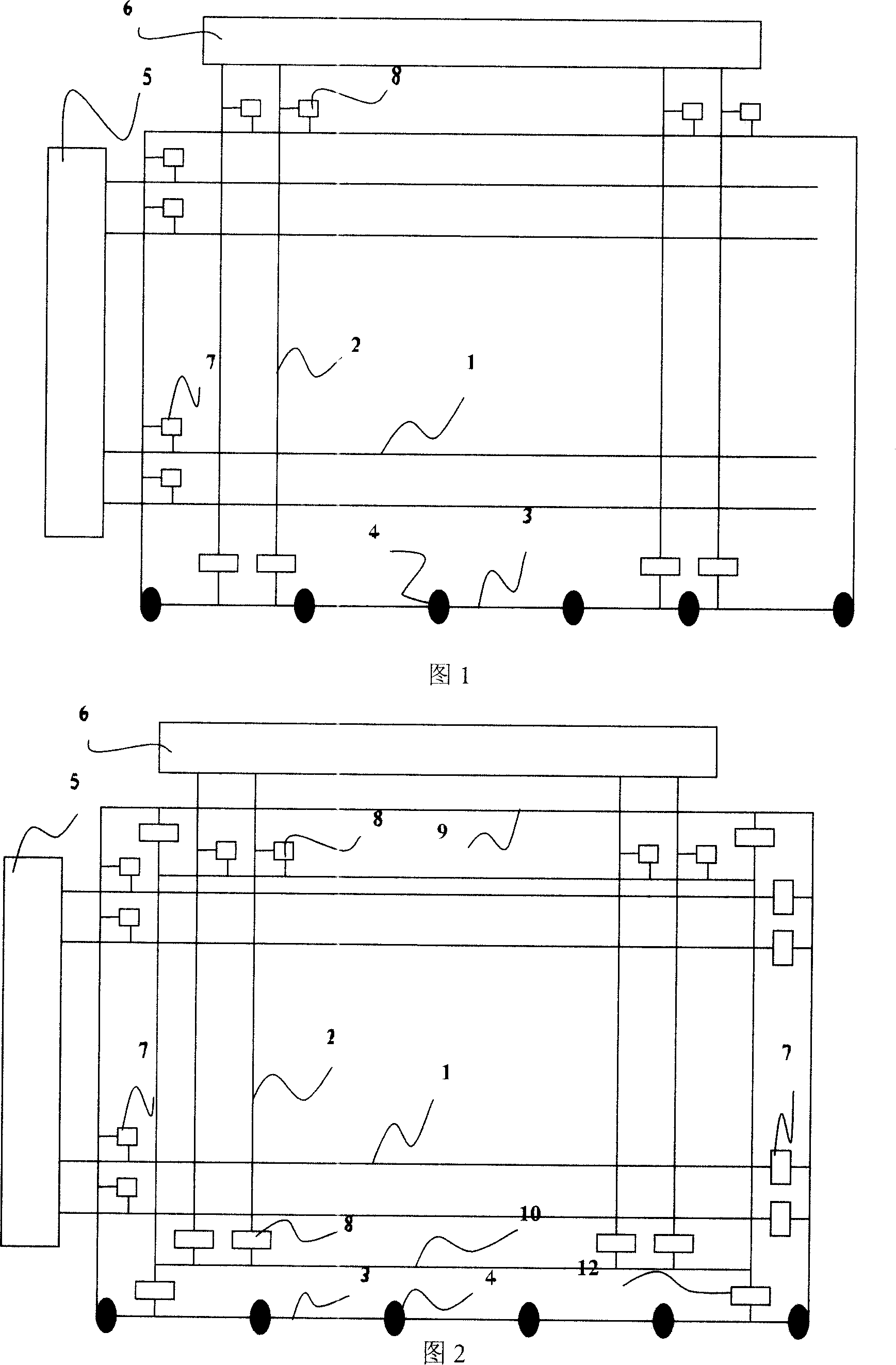
[0033] FIG. 2 is a schematic diagram of an electrostatic discharge protection circuit used in the TFT LCD of the present invention. The electrostatic damage protection circuit is formed on a substrate having a group of gate lines 1 and data lines 2 crossing the gate lines. It includes a gate line short-circuit ring 9 and a data line short-circuit ring 10, which are formed near the position of the gate electrode lead pad 5 and the source electrode lead pad 6, both of which receive common electrode signals. A set of first electrostatic discharge protection devices 7 connects both the front end and the rear end of the gate line to the gate line short-circuit ring 9 . A set of second ESD protection devices 8 connects the front end and rear end of the data line to the data line short-circuit ring 10 . The gate line short ring 9 and the data line short ring 10 are connected through a third electrostatic discharge protection device 12 . The gate line short ring 9 is directly connec...
Embodiment 2
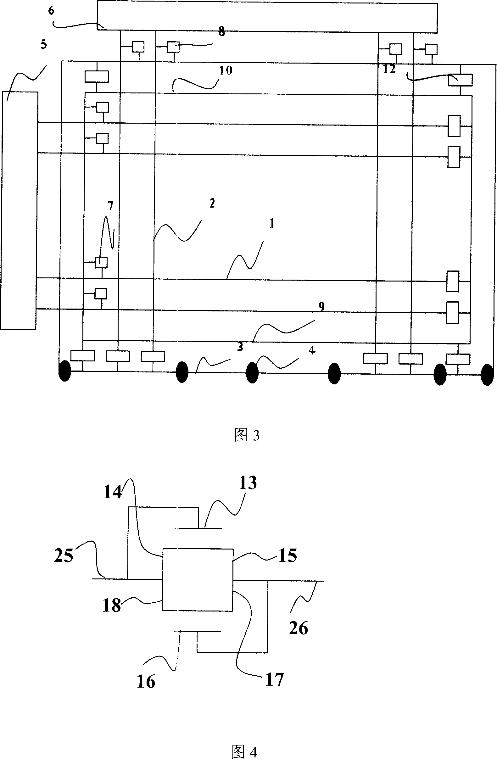
[0040] Fig. 3 is a schematic circuit diagram of another specific embodiment of the present invention. Similar to the former, it also uses two kinds of short-circuit rings, the gate line short-circuit ring 9 and the data line short-circuit ring 10 . The gate line 1 is connected to the gate line short-circuit ring 9 through the first electrostatic discharge protection device 7; the data line 2 is connected to the data line short-circuit ring 10 through the second electrostatic discharge protection device 8; the gate line short-circuit ring 9 and the data line short-circuit ring 10 They are connected through the third electrostatic discharge protection device 12 . The difference is that the data line short-circuit ring 10 directly forms the common electrode wiring, and the gate line short-circuit ring 9 is connected to the common electrode through the third electrostatic discharge protection device 12 . It works the same way as before.
[0041] The first, second and third elect...
Embodiment 1
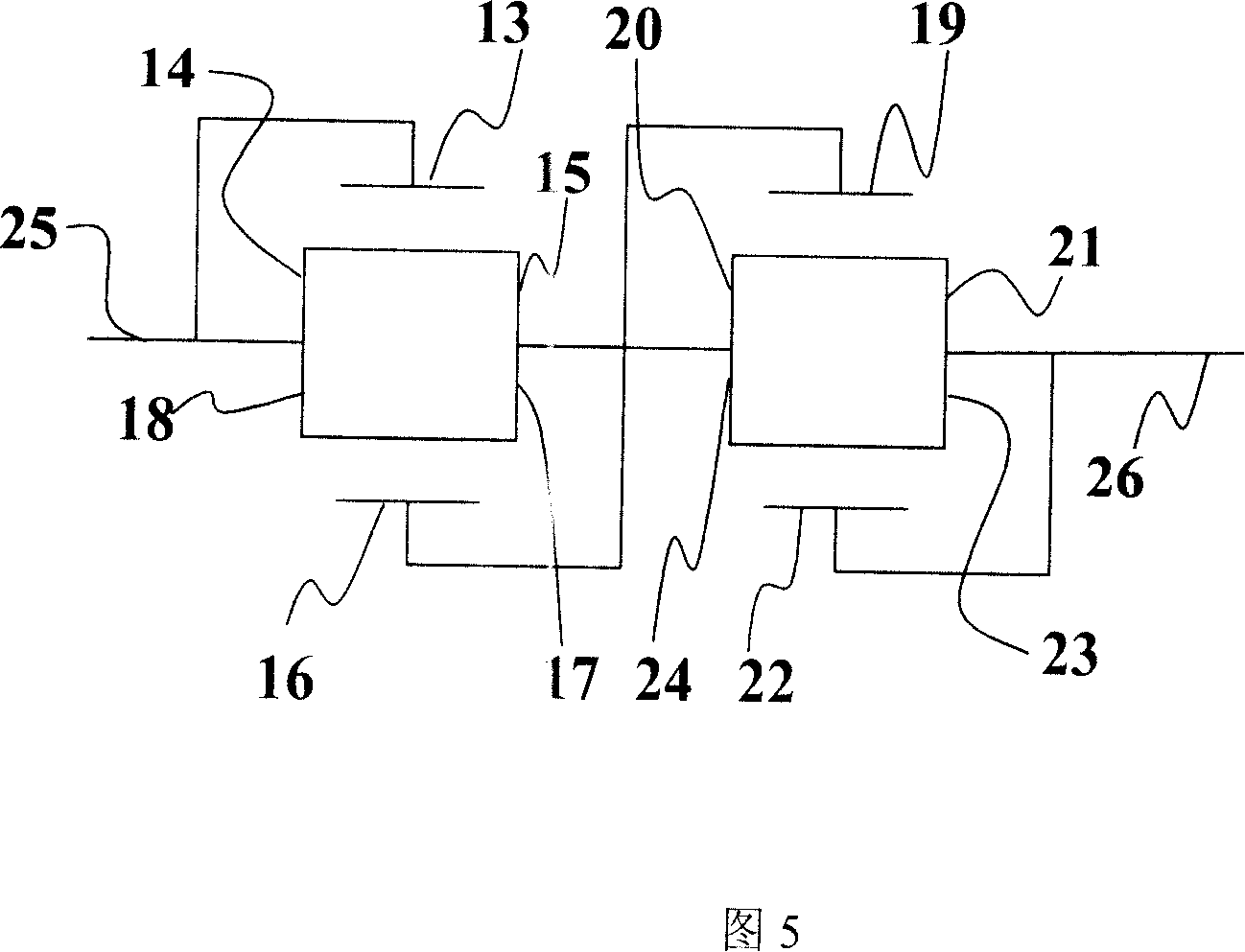
[0043] FIG. 4 is a schematic circuit diagram of a specific embodiment of an electrostatic damage protection device. The electrostatic damage protection device includes thin film transistors, which can be formed simultaneously with the TFTs of the array substrate. As shown in the figure, this electrostatic damage protection circuit consists of two thin film transistors. The gate electrode 13 of the first thin film transistor and the source electrode 14 of the first thin film transistor are connected together to form the first external lead 25 of the electrostatic damage protection device. At the same time, the drain electrode 18 of the second TFT is connected to the source electrode 14 of the first TFT. Similarly, the gate electrode 16 of the second thin film transistor and the source electrode 17 of the second thin film transistor are connected together to form the second external lead 26 of the electrostatic damage protection device. At the same time, the drain electrode 15...
PUM
 Abstract
Description
Claims
Application Information
 - R&D
- Intellectual Property
- Life Sciences
- Materials
- Tech Scout
- Unparalleled Data Quality
- Higher Quality Content
- 60% Fewer Hallucinations
Browse by: Latest US Patents, China's latest patents, Technical Efficacy Thesaurus, Application Domain, Technology Topic, Popular Technical Reports.
© 2025 PatSnap. All rights reserved.Legal|Privacy policy|Modern Slavery Act Transparency Statement|Sitemap|About US| Contact US: help@patsnap.com