
Method for manufacturing polycrystalline silicon emitter interface layer

An emitter and interface layer technology, applied in semiconductor/solid-state device manufacturing, electrical components, circuits, etc., can solve the problems of poor uniformity of silicon wafers and the oxide layer is not very dense, and achieve easy temperature control, rapid quality, Simple process steps

Inactive Publication Date: 2008-03-05
SHANGHAI HUA HONG NEC ELECTRONICS
View PDF0 Cites 3 Cited by
  • Summary
  • Abstract
  • Description
  • Claims
  • Application Information

AI Technical Summary

Problems solved by technology

The oxide layer formed on the surface of this method is not very dense, and the uniformity in the silicon wafer is not good

Method used


Image

  • Method for manufacturing polycrystalline silicon emitter interface layer
  • Method for manufacturing polycrystalline silicon emitter interface layer

Examples


Embodiment 1

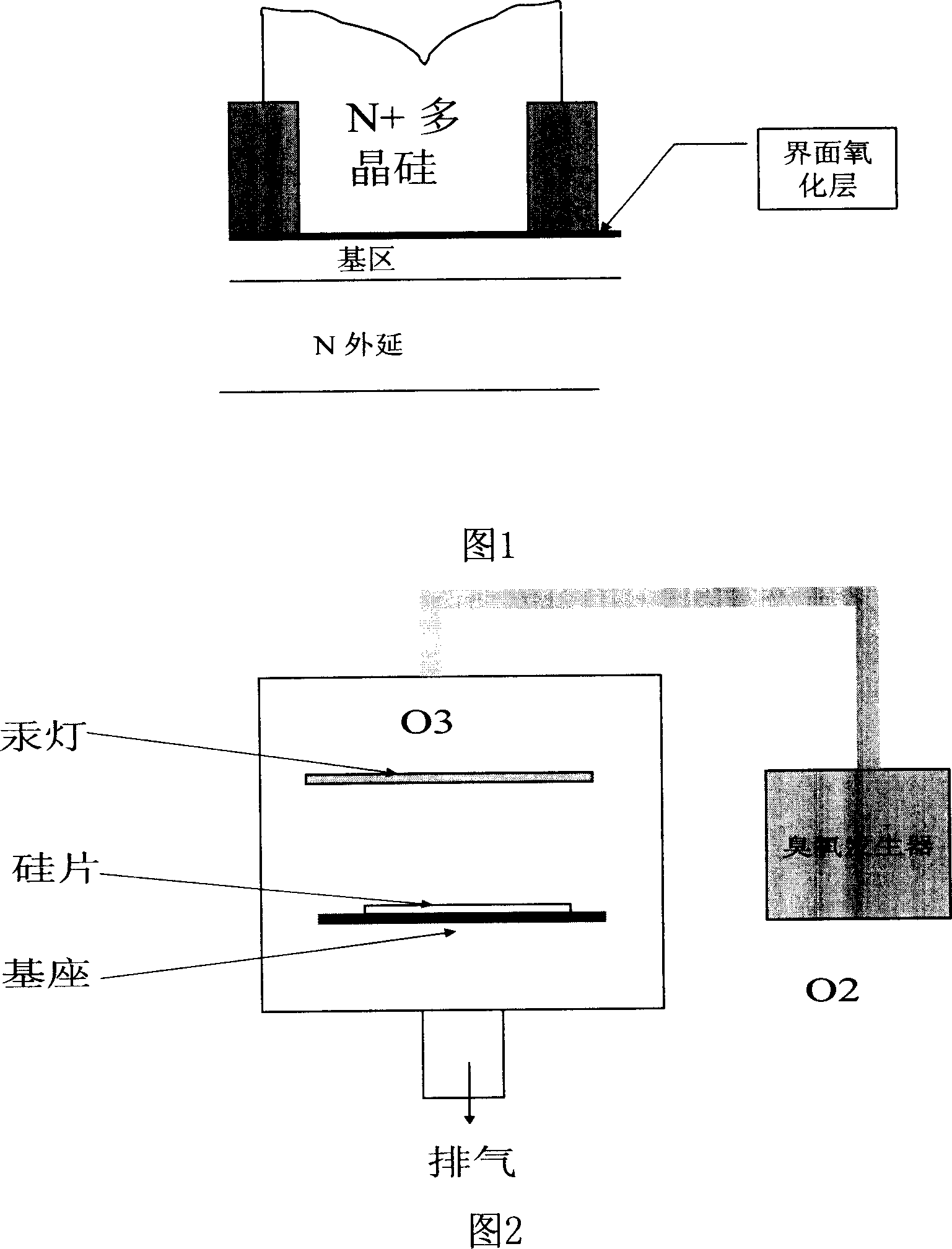
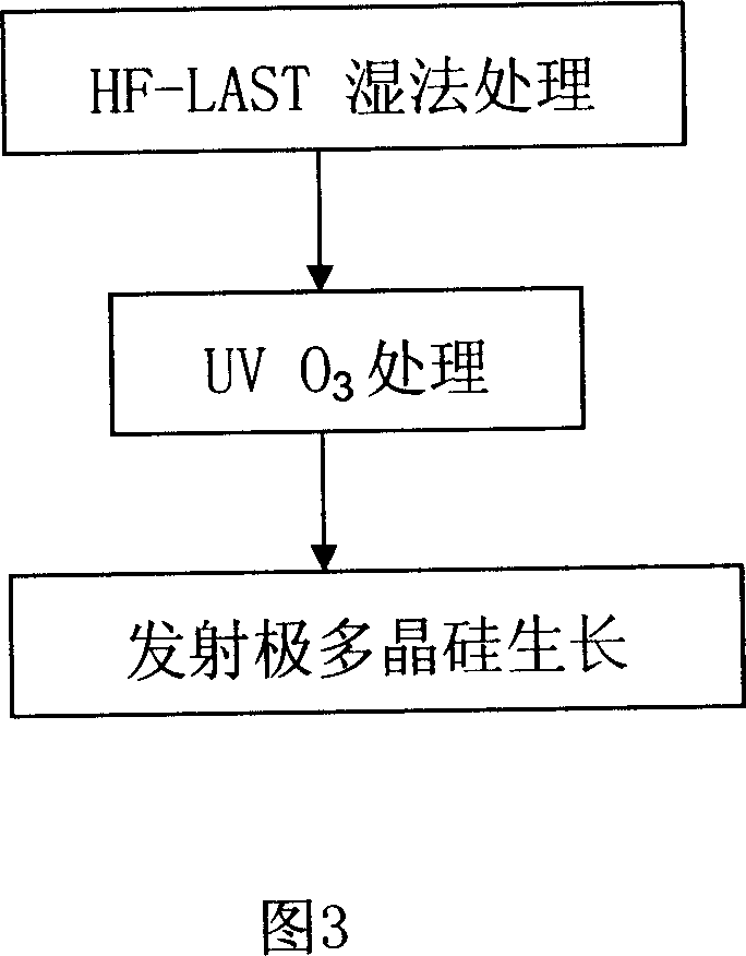
[0018] In this example, firstly, the surface of the silicon wafer is cleaned by HF-Last wet method according to the method of the present invention to ensure that the natural oxide layer on the surface is completely removed, and then the silicon wafer is placed into the UV O process as shown in Figure 2. 3 In the schematic diagram of the treatment device; the introduction of oxygen as shown in Figure 2 UV O 3 processing device, the UV O 3 The ozone generator of the processing device processes oxygen to generate ozone, and the mercury lamp of the processing device heats up; in this embodiment, the temperature in the processing device is controlled at: 150-250 degrees Celsius and the processing time is 8 minutes; the Bipolar polysilicon emitter interface is made by this example The oxide layer is relatively uniform and of good quality, and the thickness of the oxide layer formed in this example is 10 angstroms. The polysilicon emitter interface layer of BiCMOS can also be made ...


PUM


Abstract

This invention discloses a method for preparing an interface layer of a polysilicon emitter, which first of all cleans the surface of the silicon chip with a HF-Last wet method to eliminate a natural oxidation layer on the surface of the chip completely, then putting the chip into an UV03 process device to form an interface oxidation layer in a period of time under a certain temperature to process an interface layer of polysilicon emitter of Bipolar or BiCMOS, in which, the temperature is better at 100-300deg.C, the time is 1-10min. and thickness of the oxidation layer of the interface layer is 5-15.

Description

technical field [0001] The invention relates to a semiconductor manufacturing process, in particular to a method for making a polysilicon emitter interface layer Background technique [0002] When making a Bipolar or BiCMOS polysilicon emitter, it is usually necessary to form a very thin interface oxide layer between the emitter polysilicon and the base region, so that the current gain of the device is doubled, as shown in Figure 1. At present, there are mainly the following methods to generate the interface oxide layer: [0003] 1. Place it at room temperature for a long time to form a natural oxide film. This method takes a long time, and the oxide film formed in the natural atmosphere contains more impurities such as carbon and is not dense. [0004] 2. Use RCA wet solution to treat the surface to form an oxide layer on the surface. The oxide layer formed on the surface of this method is not very dense, and the uniformity in the silicon wafer is not good. [0005] 3. ...

Claims


Application Information

Patent Timeline
Patent Type & Authority Applications(China)
IPC IPC(8): H01L21/331H01L21/316
Inventor 王剑敏
Owner SHANGHAI HUA HONG NEC ELECTRONICS
Learn More