Micro-optical collector structure and manufacturing method thereof
A condensing lens and micro-bump technology, applied in optics, lenses, optical components, etc., can solve the problems of cracking, vulnerability to external environment, low hardness of organic materials, etc., and achieve the effect of reducing distance, reducing cost, and high anti-blocking ability.
- Summary
- Abstract
- Description
- Claims
- Application Information
AI Technical Summary
Problems solved by technology
Method used
Image
Examples
Embodiment Construction
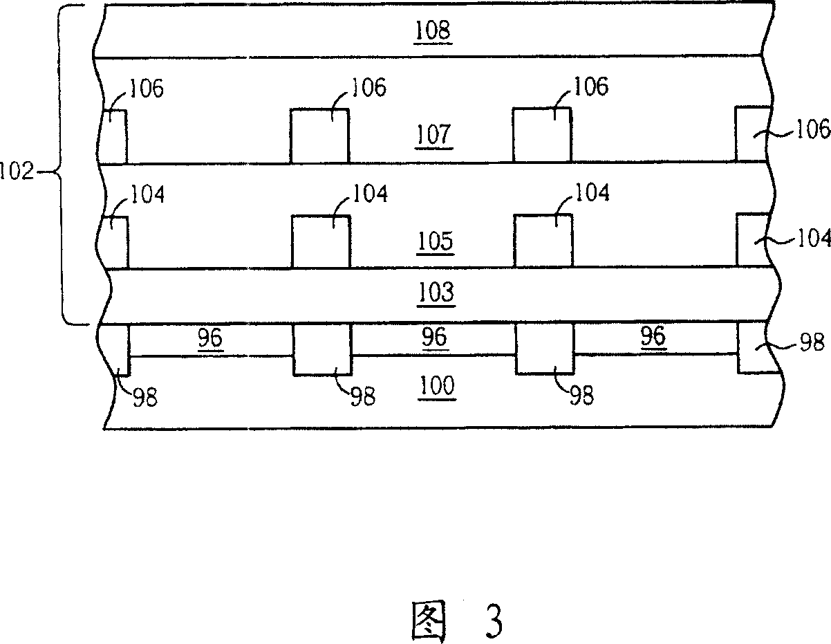
[0042]Please refer to FIG. 3 to FIG. 8 . FIG. 3 to FIG. 8 are structural cross-sectional schematic diagrams illustrating in detail the steps of the manufacturing method of the first preferred embodiment of the present invention. As shown in FIG. 3 , the present invention firstly provides a substrate 100 with a dielectric layer 102 on the substrate 100 . Wherein, the substrate 100 is a semiconductor substrate, but not limited to a silicon wafer (wafer) or a silicon-on-insulator (SOI) substrate, and the substrate 100 may include a plurality of photosensitive structures 96, such as photodiodes (photodiodes). ), etc., are used to receive external light and sense the intensity of light, and these photosensitive structures are further electrically connected to a CMOS transistor (not shown) such as a reset transistor, a current draw element or a column selection switch, and a plurality of The insulator 98, such as shallow trench isolation (shallow trench isolation, STI) or local oxid...
PUM
 Abstract
Description
Claims
Application Information


