Power luminous diode packaging structure

A technology of light-emitting diodes and packaging structures, which is applied to electrical components, electric solid-state devices, circuits, etc., can solve the problems of complex manufacturing process, unsatisfactory heat dissipation effect, and high production cost, and achieves low cost of accessories, improved heat dissipation effect and cost. low effect

Active Publication Date: 2008-03-12
FOSHAN NATIONSTAR OPTOELECTRONICS CO LTD
View PDF2 Cites 12 Cited by
  • Summary
  • Abstract
  • Description
  • Claims
  • Application Information

AI Technical Summary

Problems solved by technology

However, with the expansion of the production scale of power light-emitting diodes and the further promotion of the application field, the product structure with the patent number "US6274924" has complex manufacturing processes and low efficiency.
The thermal resistance of ceramic-based devices is relatively large, the heat dissipation effect is not ideal, and there is little space for further reducing thermal resistance, and the production cost is high

Method used


Image

  • Power luminous diode packaging structure
  • Power luminous diode packaging structure
  • Power luminous diode packaging structure

Examples


preparation example Construction

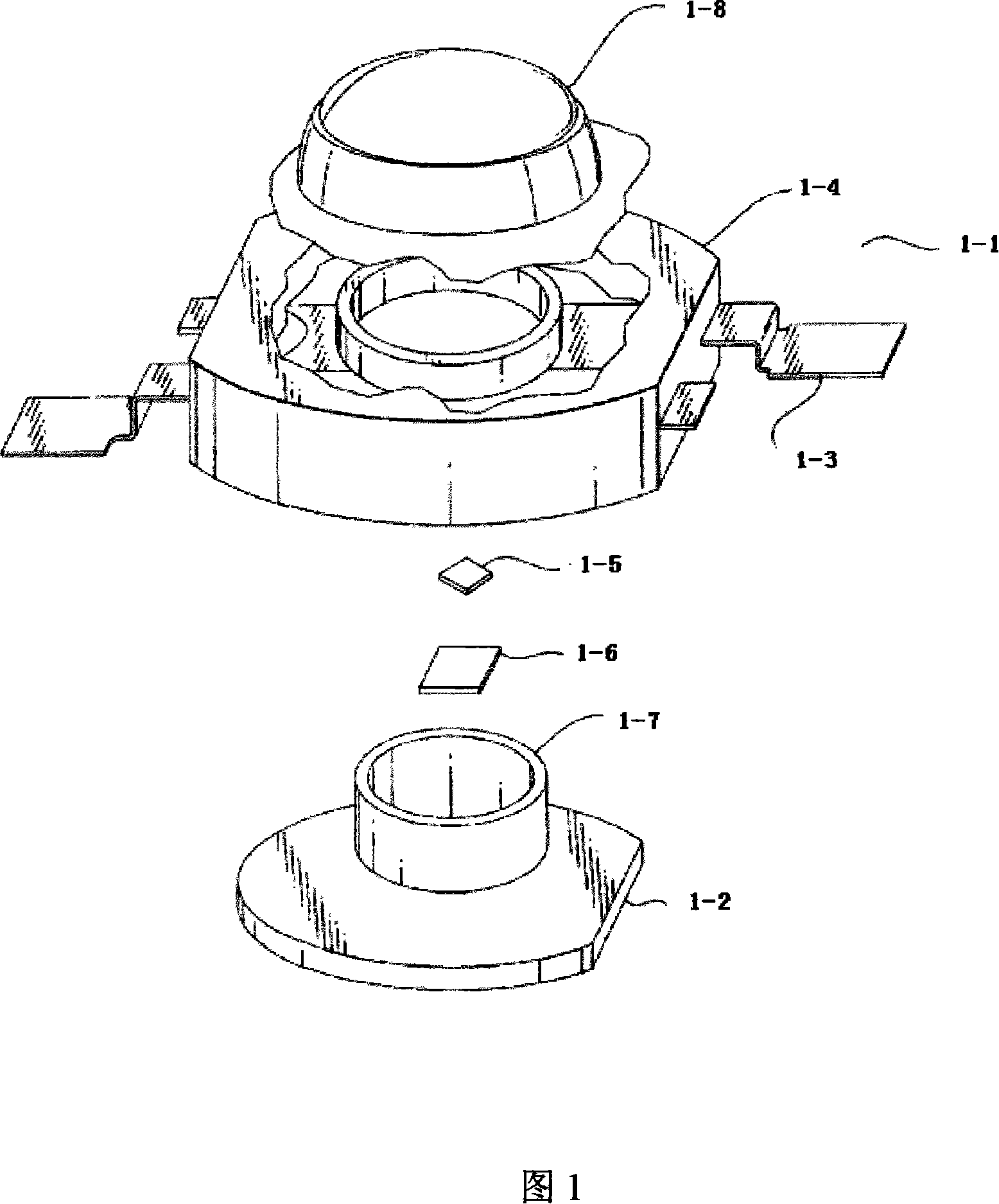
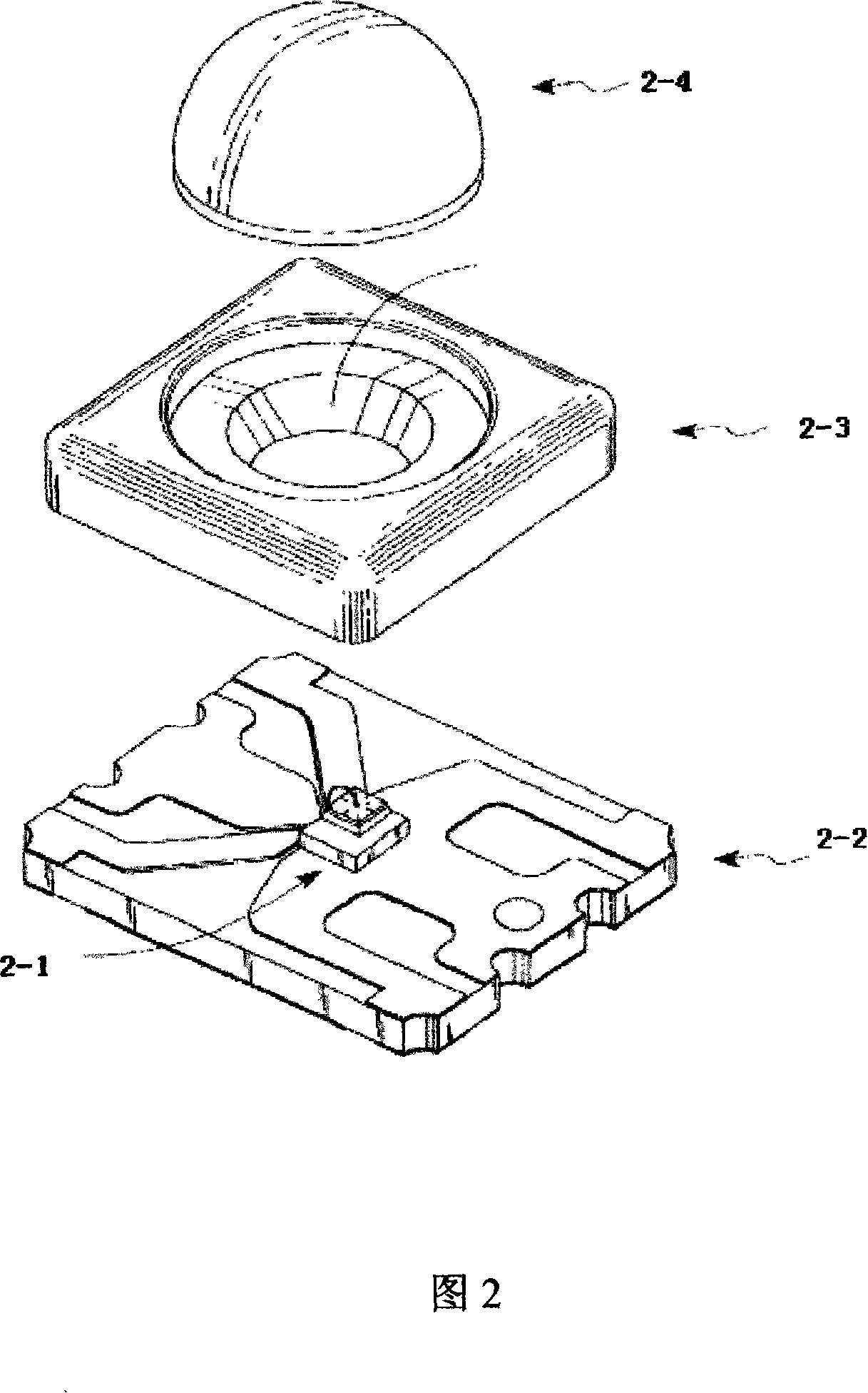
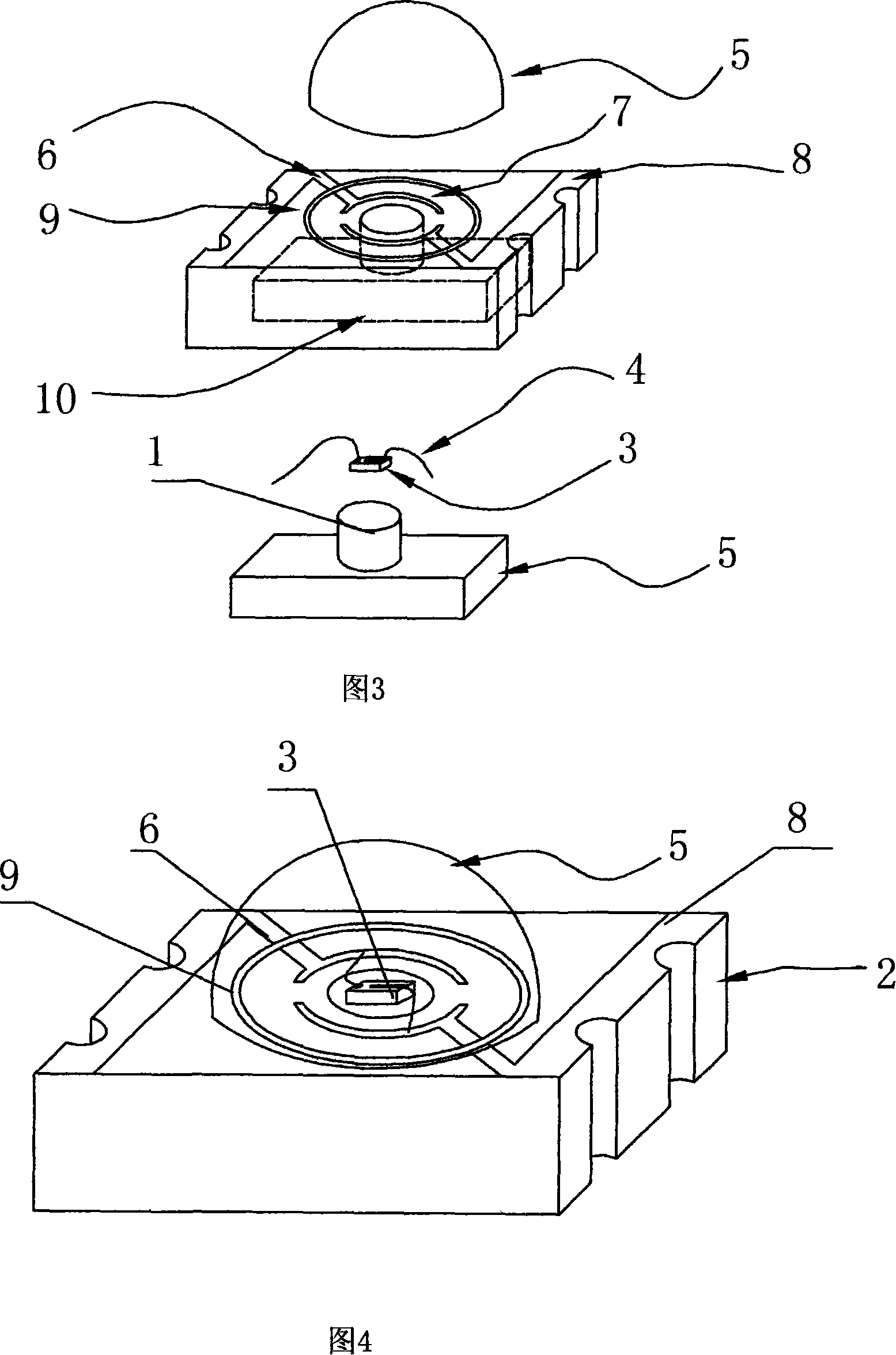
[0037] 1) Preparation of the circuit board: complete the circuit corrosion on the surface of the circuit board 2, the circuit is divided into metal circuit 6, internal metal electrode 7, external metal electrode 8 several parts, internal metal electrode 7 and external metal electrode 8 are connected through metal circuit 6, Then the choke ring 9 on the surface of the circuit board is prepared, and the choke ring 9 surrounds the upper surface of the heat sink 1 on which the LED chip 3 is placed and the internal electrodes 7 .

[0038] 2) Preparation of the counterbore structure: the machining of the counterbore structure 10 is completed through the hole forming process of the circuit board.

[0039] 3) Preparation of the heat sink: the forming of the heat sink 1 is completed.

[0040] 4) Assembly: the heat sink 1 is embedded inside the counterbore structure 10 of the circuit board 2 .

[0041] 5) Chip placement: the chip 3 is placed on the heat sink 1 .

[0042] 6) Lead conne...

Embodiment 2

[0045] The implementation example 2 of the power light-emitting diode structure of the present invention is as follows:

Embodiment 110,1。 Embodiment Synthetic ,, 1 ,,。 Embodiment approach

[0048] 1) Preparation of the upper circuit board: after the circuit printing of the upper circuit board 11 is completed, the through-hole structure 12 is prepared.

[0049] 2) Preparation of the lower circuit board: after the circuit printing of the lower circuit board 13 is completed, the through-hole structure 12' is prepared, and the through-hole has an inverted tapered structure.

[0050] 3) Heat sink preparation: complete the forming of the heat sink 1'.

[0051] 4) Assembly: sandwich the heat sink between the upper and lower circuit boards 11, 13, and then compound the two circuit boards together. The lower surface of the upper circuit board and the upper surface of the lower circuit board have electrodes connected to each other.

[0052] As a further illustration of this example, the heat sink is a circular, elliptical, square, or rectangular terraced structure. Figure 7 and Figure 8 respectively list different heat sink structures with the lower half being circular or e...


PUM


Abstract

The invention discloses a power LED encapsulation structure, which comprises a thermal sink, a breadboard, an LED chip, an internal lead and an encapsulation colloid. The thermal sink is embedded inside the countersunk structure of breadboard; the LED chip is positioned on the thermal sink; the bottom of thermal sink is directly contacted with the exterior. LED chip and breadboard down-lead electrode are connected by internal lead, while the encapsulation colloid covers the internal lead and LED chip. The invention provides a power LED encapsulation structure characterized in good heat emission, high production efficiency and low cost, which can be widely applied in lighting products based on LED.

Description

technical field [0001] The patent of the present invention relates to a power light emitting diode packaging structure, in particular to a power light emitting diode packaging structure with good heat dissipation effect, high production efficiency and low cost, which can be widely used in various LED-based lighting products. Background technique [0002] After triggering the microelectronics revolution, semiconductor technology is gestating a new industrial revolution—the lighting revolution. In 5 to 10 years, solid-state lighting using light-emitting diodes (LEDs) as new light sources will gradually appear in every corner of the traditional lighting market. In terms of device packaging structure, the world's major LED manufacturers have successively launched various power LED packaging structure products. [0003] The patent named "SURFACE MOUNTABLE LEDPACKAGE" and the patent number "US6274924" applied by Lumileds Company of the United States introduced a high-power LED pa...

Claims


Application Information

Patent Timeline
Patent Type & Authority Applications(China)
IPC IPC(8): H01L33/00H01L23/498H01L23/367H01L33/48H01L33/64
CPCH01L33/642H01L33/483H01L2224/48091H01L2924/00014H01L33/64
Inventor 余彬海李军政夏勋力
Owner FOSHAN NATIONSTAR OPTOELECTRONICS CO LTD
Why Eureka
Try Eureka