Interleaved three-dimensional on-chip differential inductors and transformers

A three-dimensional chip, interleaved technology, applied in variable inductor/transformer, inductor/transformer/magnet manufacturing, inductors, etc., can solve problems such as limiting the self-resonant frequency of on-chip inductors and transformers

Inactive Publication Date: 2008-03-12
RGT UNIV OF CALIFORNIA
View PDF3 Cites 14 Cited by
  • Summary
  • Abstract
  • Description
  • Claims
  • Application Information

AI Technical Summary

Problems solved by technology

In substrate-lossy silicon-based integrated circuits, it is especially important to fabricate on-chip inductors and transformers with as small a real area as possible, because the large area of ​​the inductor/transformer induces a large gap between the on-ch

Method used


Image

  • Interleaved three-dimensional on-chip differential inductors and transformers
  • Interleaved three-dimensional on-chip differential inductors and transformers
  • Interleaved three-dimensional on-chip differential inductors and transformers

Examples


Embodiment Construction

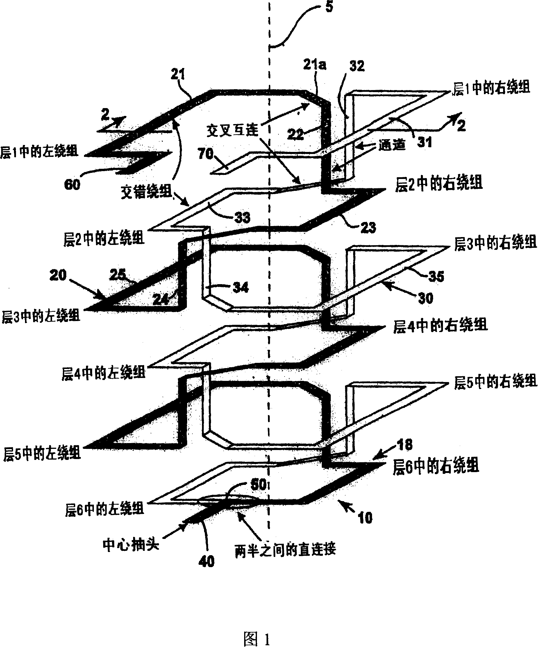
[0037] Various interleaved 3D on-chip differential inductors and transformers are provided according to the present invention.

[0038]The interleaved 3D on-chip differential inductors and interleaved on-chip transformers are well known to those skilled in the art such as complementary metal oxide semiconductor (CMOS), bipolar transistor and integration of CMOS technologies (BiCMOS), and Manufactured with standard processes in silicon-germanium (SiGe) technology.

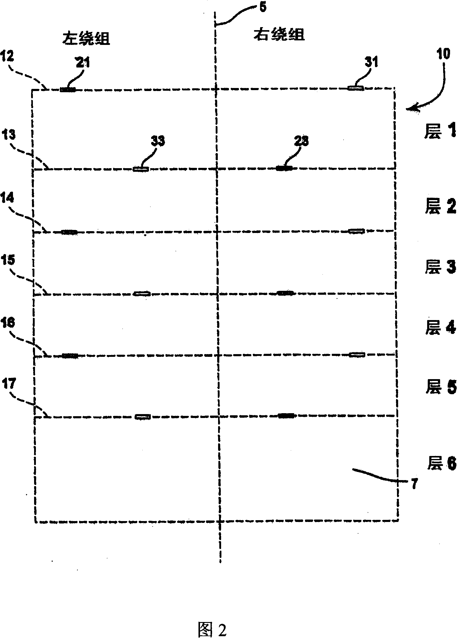
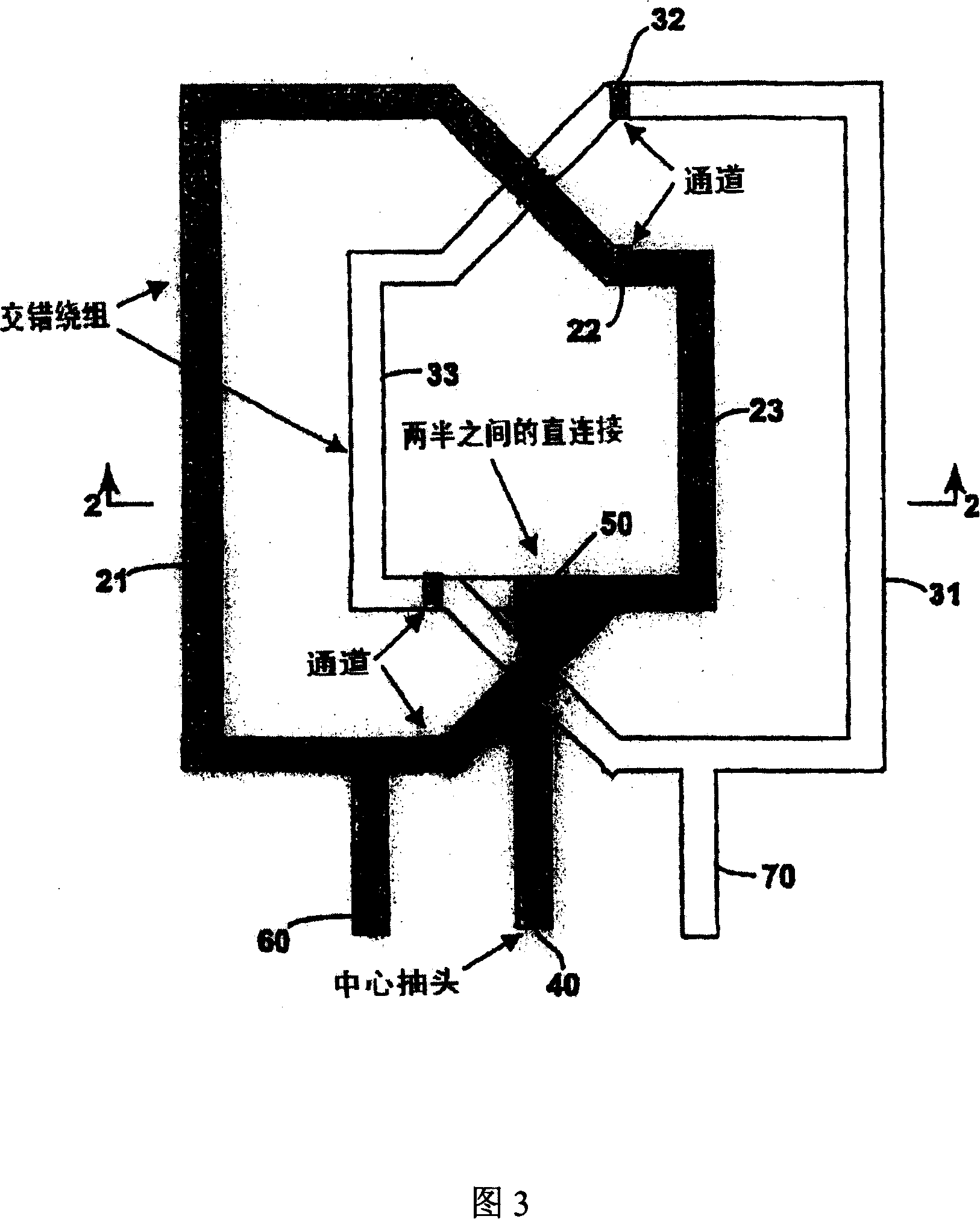
[0039] The interleaved 3D on-chip differential inductors and interleaved on-chip transformers described below were fabricated as multiple layers comprising windings. The layers of the winding are patterned, deposited or otherwise disposed on the layers as they are created. The windings between the layers are interconnected by vias.

[0040] FIG. 1 shows a perspective view of a preferred embodiment of an interleaved on-chip differential inductor, generally designated reference numeral 10 . 2 and 3 respectively sho...


PUM


Abstract

Interleaved three-dimensional (3D) on-chip differential inductors and transformers are disclosed. The interleaved 3D on-chip differential inductors and transformers make the best use of multiple metal layers in mainstream standard processes, such as CMOS, BiCMOS and SiGe technologies.

Description

[0001] Cross-references to related applications [0002] This application claims the Serial titled "Interleaved 3D On-Chip Differential Inductor and Transformer" filed Aug. 4, 2005 by Daquan Huang and Mau-Chung F. Chang Benefit of US Provisional Patent Application No. 60 / 705,868, the disclosure of which is incorporated herein by reference for all purposes permitted by statute. [0003] Statements related to federally sponsored research and development [0004] Development of this invention was made with government support under Award No. N66001-04-1-8934 awarded by the United States Navy. The US Government has certain rights in this invention. technical field [0005] This invention relates to inductors and transformers. In particular, the present invention relates to improved on-chip inductors and transformers and methods of manufacturing the same. Background technique [0006] On-chip inductors and transformers are key passive components in radio frequency / millimeter w...

Claims


Application Information

Patent Timeline
IPC IPC(8): H01F5/00H01F27/28H01F27/29
CPCH01F17/0013H01F2021/125H01F41/041H01F2017/002Y10T29/4902
Inventor 茂春·弗兰克·张黄大泉
Owner RGT UNIV OF CALIFORNIA
Why Eureka
Try Eureka