Supercharge Your Innovation With Domain-Expert AI Agents!

Bipolar transistor and method of fabricating the same

A bipolar transistor and base technology, applied in semiconductor/solid-state device manufacturing, semiconductor devices, electrical components, etc., can solve the problems of increasing the number of manufacturing steps and increasing manufacturing costs, reducing series resistance and improving high-frequency performance. Effect

Active Publication Date: 2008-03-12
NXP BV
View PDF1 Cites 6 Cited by
  • Summary
  • Abstract
  • Description
  • Claims
  • Application Information

AI Technical Summary

Problems solved by technology

Another disadvantage is the need for stacked layers in order to create the transistor opening area in which the bipolar transistor is formed, which increases the number of manufacturing steps and therefore increases the manufacturing cost

Method used


Image

  • Bipolar transistor and method of fabricating the same
  • Bipolar transistor and method of fabricating the same
  • Bipolar transistor and method of fabricating the same

Examples


Embodiment Construction

[0016] The figures are not drawn to scale. Generally, like parts are indicated by like reference numerals in the drawings.

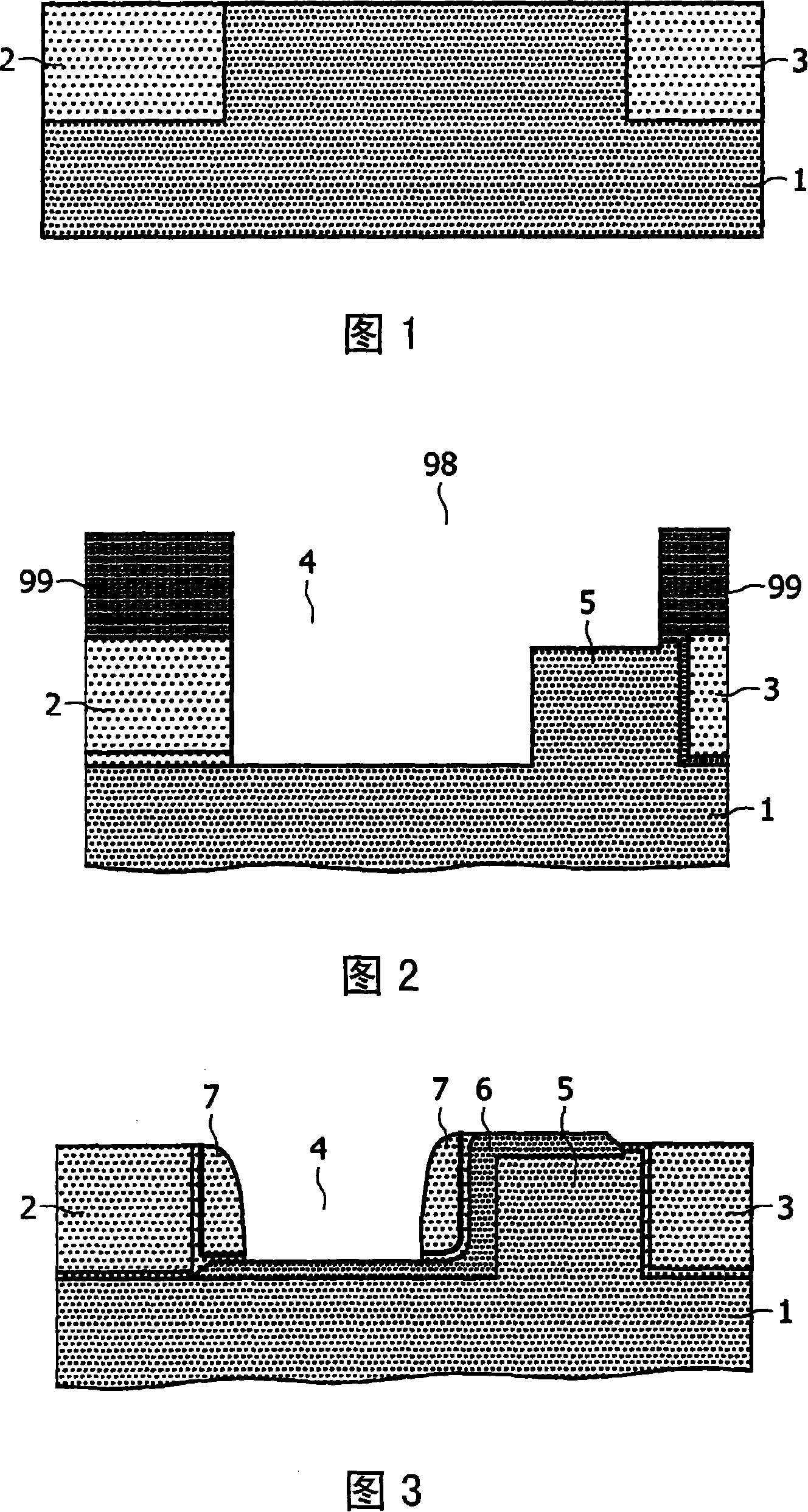
[0017] Figure 1 shows an initial structure comprising a silicon substrate 1 provided with two shallow trench isolation regions 2 and 3 fabricated using standard CMOS fabrication techniques. The shallow trench isolation regions 2 and 3 may include silicon dioxide or any other insulating material.

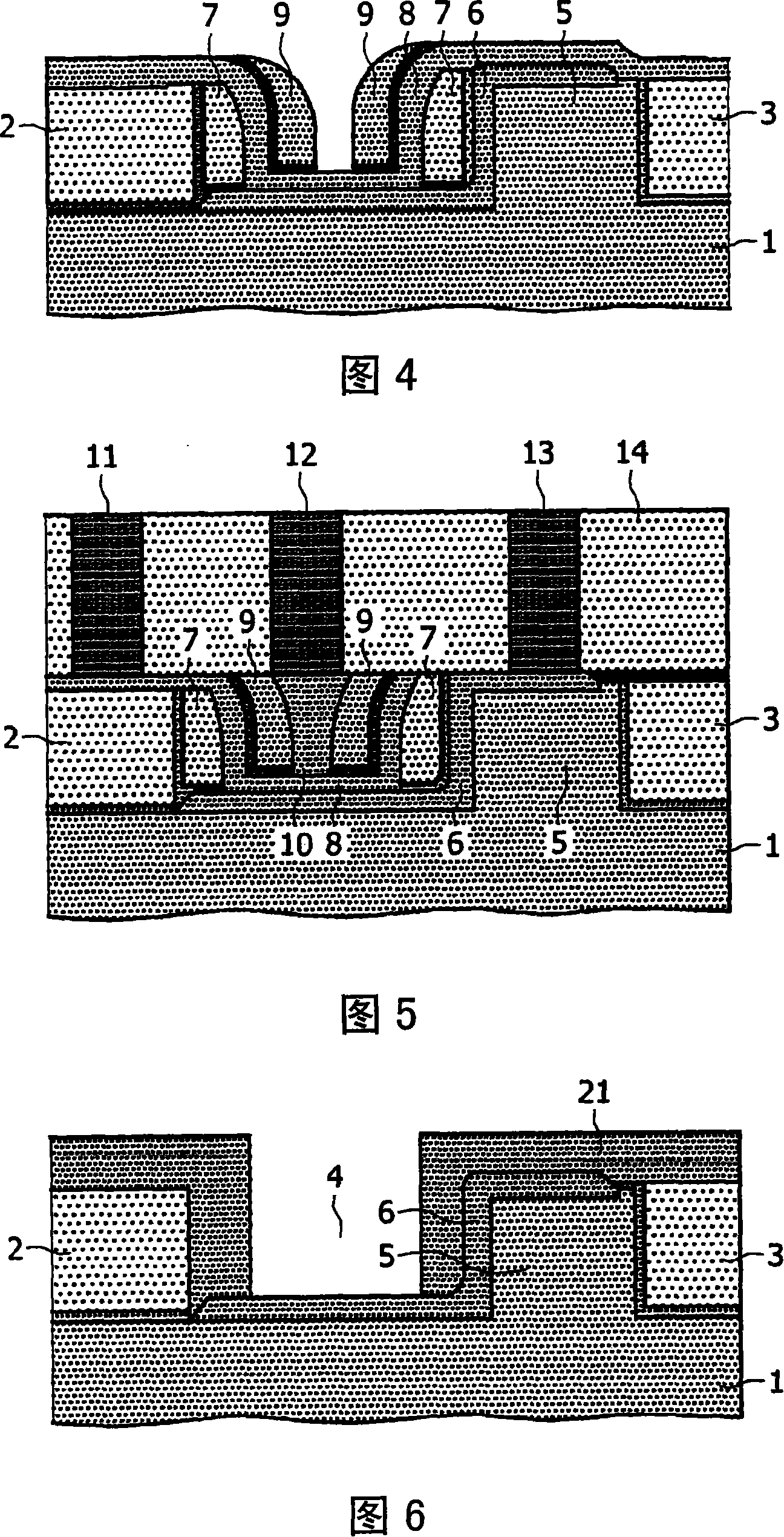
[0018] Next, as shown in FIG. 2 , a resist layer 99 is formed, and a transistor opening region 98 is formed by using photolithography technology, exposing a part of the shallow trench isolation region 2 and a part of the silicon substrate 1 . The exposed portion of the shallow trench isolation region 2 is selectively etched with respect to the silicon substrate 1 . At this time, grooves 4 and protrusions 5 are formed, and protrusions 5 contain silicon substrate 1 . The trench 4 has a first sidewall adjacent to the shallow trench isolation region 2 , a second...


PUM


Abstract

The invention provides a bipolar transistor with a reduced collector series resistance integrated in a trench (4, 44) of a standard CMOS shallow trench isolation region. The bipolar transistor includes a collector region (6, 34) manufactured in one fabrication step, therefore having a shorter conductive path with a reduced collector series resistance, improving the high frequency performance of the bipolar transistor. The bipolar transistor further includes a base region (8, 22, 38) with a first part on a selected portion of the collector region (6, 34), which is on the bottom of the trench (4, 44), and an emitter region (10, 24, 39) on a selected portion of the first part of the base region (8, 22, 38). A base contact (11, 26, 51) electrically contacts the base region (8, 22, 38) on a second part of the base region (8, 22, 38), which is on an insulating region (2, 42). The collector region (6, 34) is electrically contacted on top of a protrusion (5, 45) with a collector contact (13, 25, 50).

Description

technical field [0001] The present invention relates to bipolar transistors and methods for their manufacture. Background technique [0002] In WO 03 / 100845 a method of manufacturing a bipolar transistor is disclosed in which a substrate is provided with two shallow trench isolation regions and an insulating layer overlying the substrate. In addition, three different collector layers are provided for forming the conductive path from the collector to the substrate surface, including an N-type collector epitaxial layer between two shallow trench isolation regions, a buried collector n-layer and n plunger (plug) heat sink (sinker). A layer structure including a conductive layer is formed on the insulating layer, after which the transistor opening area is etched through the conductive layer. Afterwards, a SiGe base layer is deposited on the inner wall of the opening of the transistor region, thereby electrically connecting the SiGe base layer with the conductive layer and the ...

Claims


Application Information

Patent Timeline
Patent Type & Authority Applications(China)
IPC IPC(8): H01L21/31H01L29/732H01L29/737
Inventor 约翰内斯·J·T·M·唐克斯韦伯·D·范诺尔特菲利浦·默尼耶-贝拉德塞巴斯蒂恩·尼坦克埃尔温·海曾弗朗索瓦·纳耶莉
Owner NXP BV
Features
  • R&D
  • Intellectual Property
  • Life Sciences
  • Materials
  • Tech Scout
  • Unparalleled Data Quality
  • Higher Quality Content
  • 60% Fewer Hallucinations
Learn More