Non-contact smart card and its production method
The technology of a non-contact smart card and manufacturing method is applied in the direction of recording carriers used in machines, instruments, computer components, etc. It can solve problems such as solder joint detachment, affecting antenna conductivity, failure, etc., to reduce chip damage rate, Improvement of product yield and improvement of bending resistance
- Summary
- Abstract
- Description
- Claims
- Application Information
AI Technical Summary
Problems solved by technology
Method used
Image

Examples
Embodiment Construction
[0031] The present invention will be further described below in conjunction with accompanying drawing.
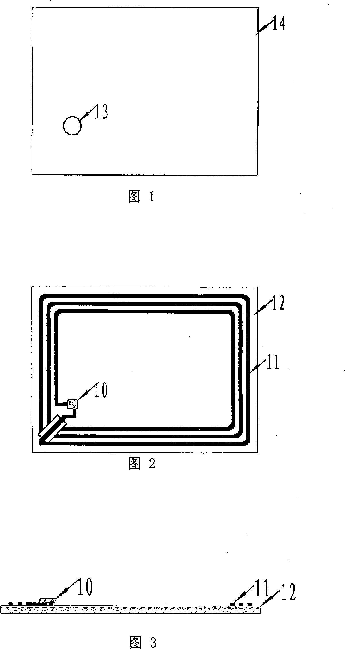
[0032] A kind of non-contact smart card of the present invention comprises polymer base layer 12, filling layer 14; The polymer base layer 12 is provided with etching antenna 11 and chip 10, and the chip hole 13 on the filling layer 14 just covers the chip of polymer base layer 12 10 , the thickness of the filling layer 14 is greater than or equal to the thickness of the chip 10 , as shown in FIG. 1 , FIG. 2 and FIG. 3 .
[0033] The method for making the contactless smart card can use a commercially available flip chip machine.
[0034] First, the reverse chip process is performed. The polymer film carrying the etched antenna 11 is mounted on a flip-chip machine. Apply opposite-sex conductive glue on the bonding position on the antenna, remove the chip 10 from the wafer and fill it in the bonding position; then pressurize and heat the chip 10 up and down to make the cond...
PUM
 Abstract
Description
Claims
Application Information