System for generating plasma body

A plasma and coil technology, applied in the field of semiconductor manufacturing, can solve the problems affecting the flattening effect of the wafer, weak plasma energy, etc., and achieve the effects of consistent etching and deposition rates, increased electromagnetic field strength, and reduced energy loss.

Inactive Publication Date: 2008-04-02
SEMICON MFG INT (SHANGHAI) CORP
View PDF1 Cites 2 Cited by
  • Summary
  • Abstract
  • Description
  • Claims
  • Application Information

AI Technical Summary

Problems solved by technology

Due to the energy difference between the plasma central region and the edge region, the plasma energy at the edge of the wafer is relatively weak. As the deposition and etching processes alternate, the material filled and etched away at the edge of the wafer is less than that of the wafer. Central area, therefore, after the trench is filled, a peak 400 as shown in Figure 2E will appear in the wafer edge area, which will affect the subsequent wafer planarization effect

Method used


Image

  • System for generating plasma body
  • System for generating plasma body
  • System for generating plasma body

Examples


Embodiment Construction

[0034] In order to make the above objects, features and advantages of the present invention more comprehensible, specific implementations of the present invention will be described in detail below in conjunction with the accompanying drawings.

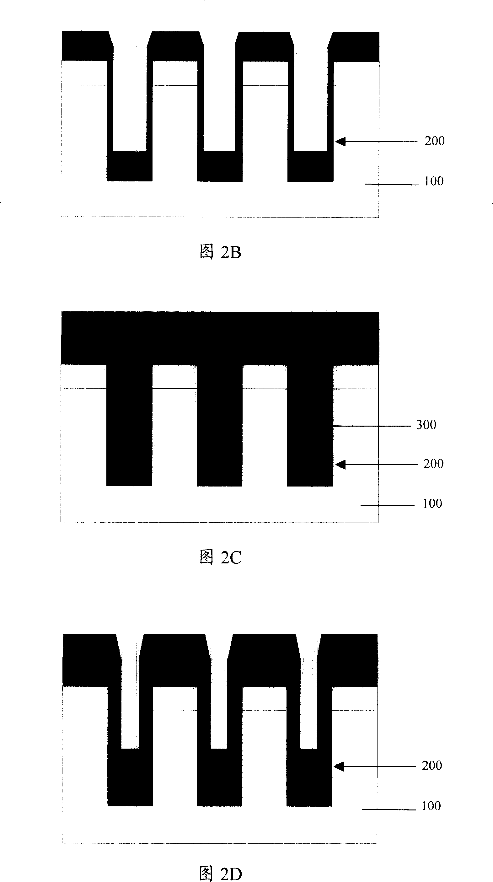
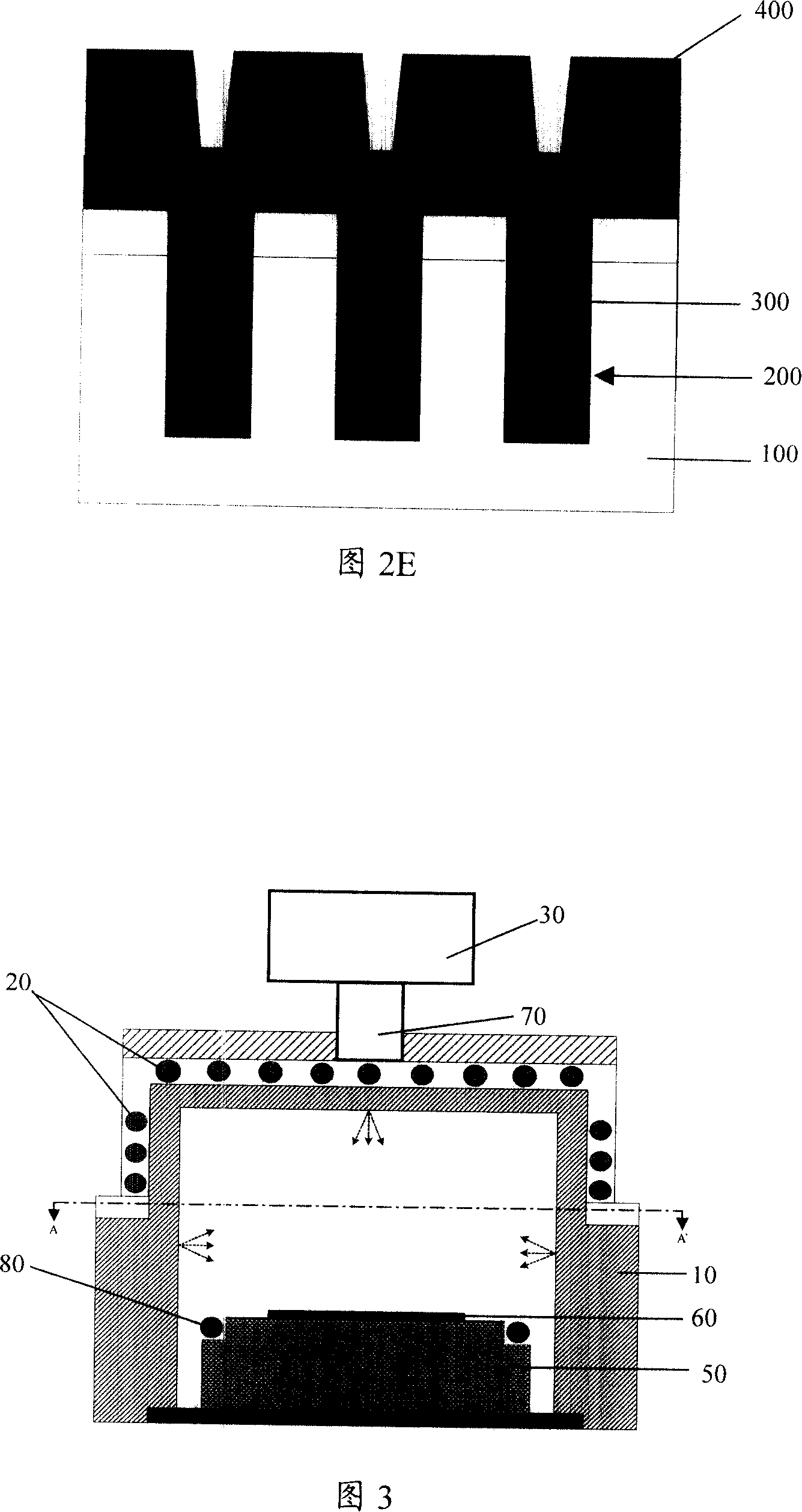
[0035] The invention relates to the technical field of semiconductor integrated circuit manufacturing, in particular to a method for forming a shallow trench isolation structure in a semiconductor device and the shallow trench isolation structure. It should be noted here that this specification provides different embodiments to illustrate the various features of the present invention, but these embodiments are only for convenience of description by using specific compositions and structures, and do not limit the present invention.

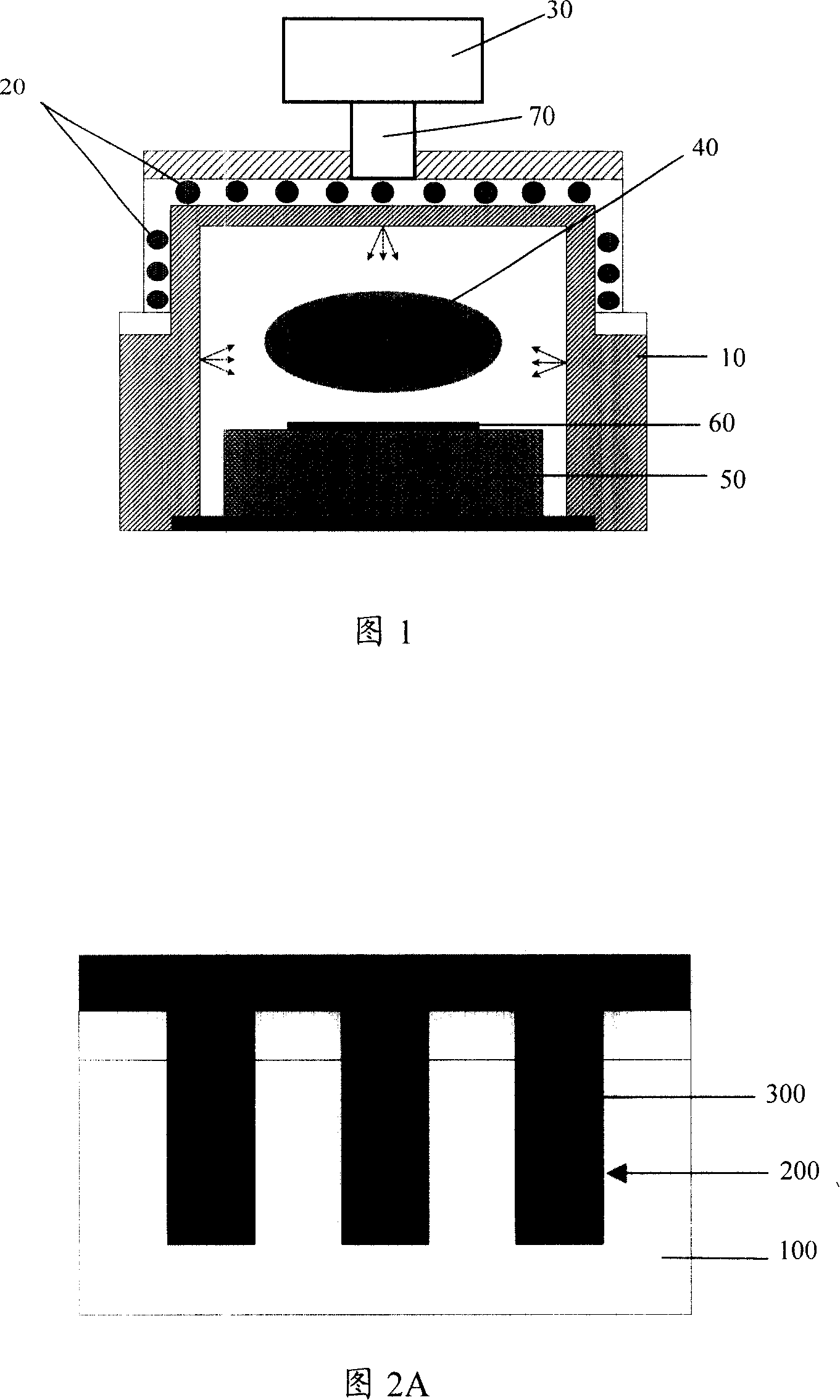
[0036] FIG. 3 is a simplified schematic diagram of a system structure for generating plasma according to an embodiment of the present invention. The schematic diagram is just an example, which should not li...


PUM

PropertyMeasurementUnit
Drive currentaaaaaaaaaa

Abstract

A system for generating plasma of the invention includes reaction chamber; wafer chuck disposed in the reaction chamber; a first coil on the upper and top of the reaction chamber; radio frequency power source which output radio frequency current to incite the first coil to generate plasma; and a second coil disposed on the lower of the reaction chamber. The system of the invention for generating plasma can generate more homogeneous plasma.

Description

technical field [0001] The invention relates to the technical field of semiconductor manufacturing, in particular to a system for generating plasma. Background technique [0002] Plasma is used extensively in semiconductor manufacturing processes. Plasma is usually generated in a low-pressure environment. The reaction gas is introduced into the reaction chamber and the electron flow is introduced, and the electrons are accelerated by a radio frequency (RF) electric field, so that the electrons collide with the gas molecules and transfer kinetic energy, thereby ionizing the gas molecules. become plasma. The generated plasma can be used in various semiconductor manufacturing processes, such as plasma etching, deposition, etc. European Patent Application No. 95307268.3 discloses a system for generating plasma. Fig. 1 is a simplified schematic diagram of the existing system structure for generating plasma. As shown in Fig. 1, the system includes a reaction chamber 10, and the ...

Claims


Application Information

Patent Timeline
IPC IPC(8): H05H1/46H01L21/00
Inventor 刘明源刘乒
Owner SEMICON MFG INT (SHANGHAI) CORP
Why Eureka
Try Eureka