Optical sensor, solid-state imaging device, and operation method of solid-state imaging device

A technology of solid-state imaging device and light sensor, which is applied in electric solid-state devices, radiation control devices, image communication, etc., can solve the problems of low S/N ratio, low sensitivity, damage to the quality of animation camera images, etc., and achieve high S/N ratio, high sensitivity effect

Active Publication Date: 2008-04-16
TOHOKU UNIV
View PDF4 Cites 19 Cited by
  • Summary
  • Abstract
  • Description
  • Claims
  • Application Information

AI Technical Summary

Problems solved by technology

[0018] However, in the methods described in Patent Documents 1, 2, and 3 and Non-Patent Document 2 or the method of imaging with two or more different exposure times, low-illuminance imaging and high-illuminance imaging are performed at different timings. Therefore, there is a problem that there is a deviation in the recording time, which impairs the image quality of animation recording.
[0019] In addition, in the above-mentioned methods described in Patent Document 4 and Patent Document 3, although a wide dynamic range can be realized corresponding to imaging on the high-illuminance side, there is a problem in that the imaging on the low-illuminance side becomes low-sensitivity. , low S / N ratio, impairing image quality
[0020] As mentioned above, in image sensors such as CMOS image sensors, it is difficult to achieve a wide dynamic range while maintaining high sensitivity and high S / N ratio

Method used


Image

  • Optical sensor, solid-state imaging device, and operation method of solid-state imaging device
  • Optical sensor, solid-state imaging device, and operation method of solid-state imaging device
  • Optical sensor, solid-state imaging device, and operation method of solid-state imaging device

Examples


no. 1 approach

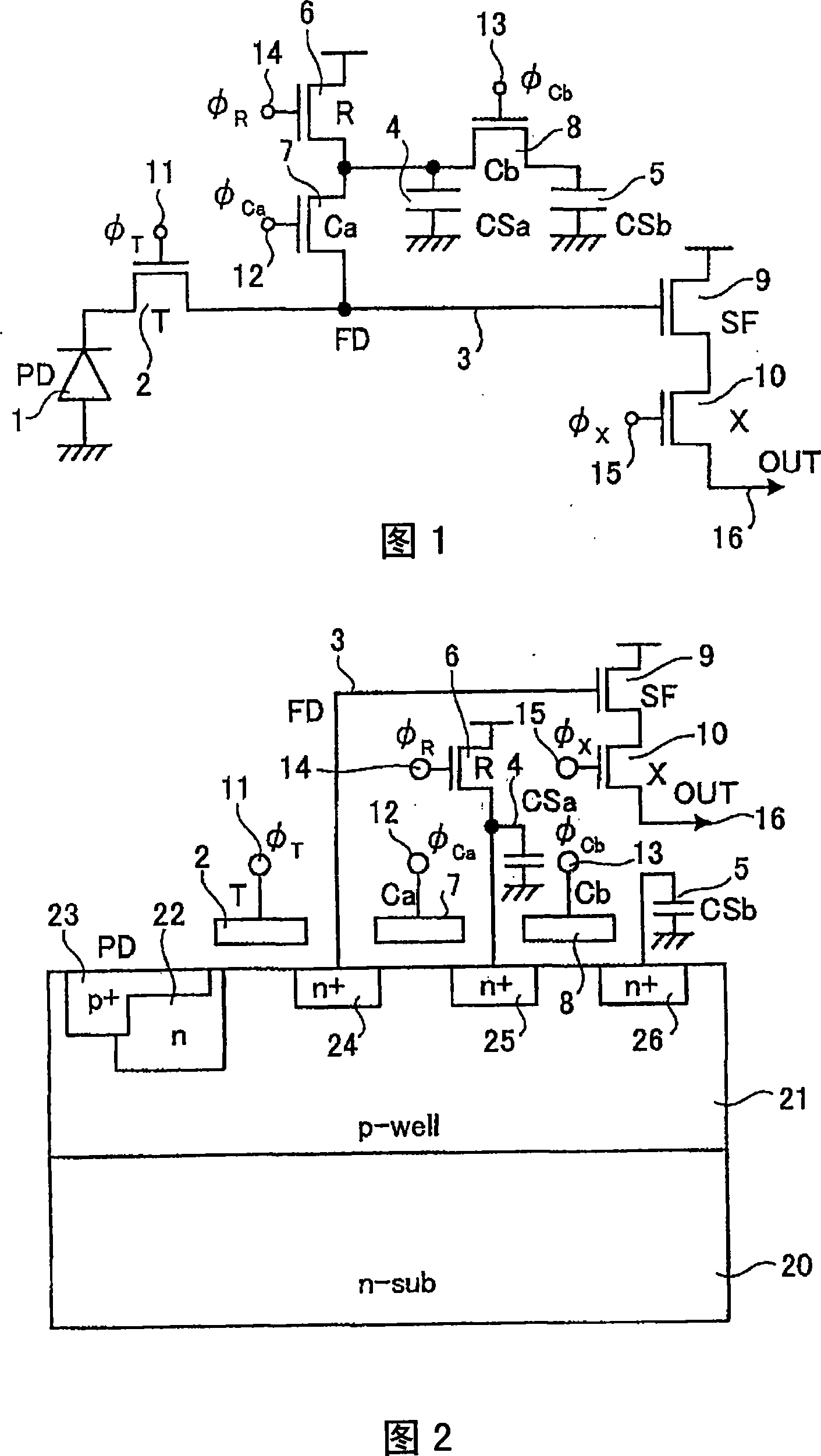
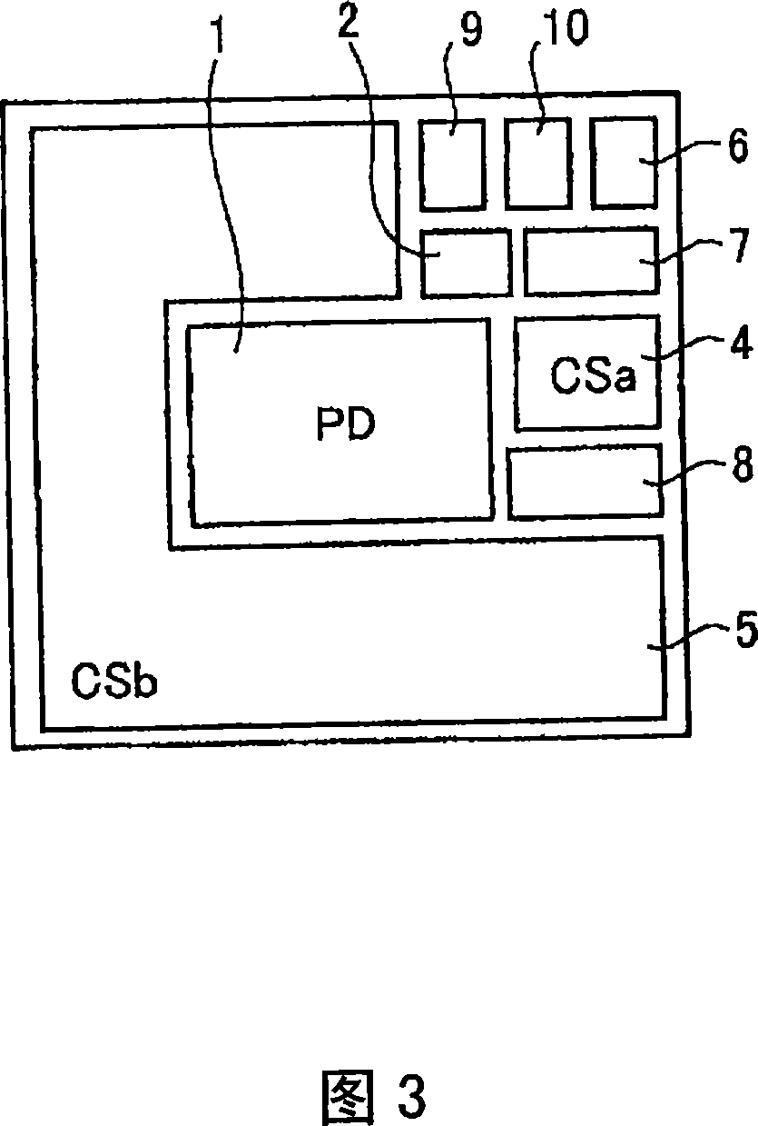
[0079] FIG. 1 shows an equivalent circuit diagram of one pixel of the solid-state imaging device according to this embodiment, FIG. 2 shows a schematic cross-sectional view, and FIG. 3 shows a schematic plan view.

[0080]Each pixel is composed of the following parts: a photodiode PD1 that receives light and generates photocharges; a transfer transistor T2 that transmits photocharges provided adjacent to the photodiode PD1; a floating diffusion FD3 that is connected to the photodiode PD1 via the transfer transistor T2; The transfer transistor T2 stores the first storage capacitor CSa4 and the second storage capacitor CSb5 of the photocharge overflowed from the photodiode PD1 during the exposure and storage operation; it is connected to the first storage capacitor CSa4 to discharge the first storage capacitor. Capacitor CSa4, second storage capacitor CSb5 and reset transistor R6 for signal charge in floating diffusion FD3; first storage transistor Ca7 arranged between floating d...

no. 2 approach

[0108] This embodiment is an embodiment of another operating method of the solid-state imaging device according to the first embodiment. The configuration of the solid-state imaging device of this embodiment is the same as that of the solid-state imaging device of the first embodiment described with reference to FIGS. 1 to 4 . However, the threshold voltage of the first storage transistor Ca and the second storage transistor Cb is lower than that of the transfer transistor T. As shown in FIG.

[0109] 8 is a main driving time chart of the solid-state imaging device according to this embodiment, and FIG. 9 is a partial schematic potential diagram from a photodiode of a pixel through a floating diffusion FD, a first storage capacitor, and a second storage capacitor.

[0110] First, before exposure and storage, the first storage transistor Ca and the second storage transistor Cb are turned on, and the transfer transistor T and reset transistor R are turned off. Next, the reset t...

no. 3 approach

[0117] FIG. 10 shows an equivalent current diagram of one pixel of the solid-state imaging device of this embodiment, and FIG. 11 shows a schematic cross-sectional view, and the schematic plan view is the same as that of FIG. 3 of the first embodiment.

[0118]Each pixel is composed of the following parts: a photodiode PD1 that receives light and generates photocharges; a transfer transistor T2 that transmits photocharges provided adjacent to the photodiode PD1; a floating diffusion FD3 that is connected to the photodiode PD1 via the transfer transistor T2; During the exposure storage operation, the first storage capacitor CSa4 and the second storage capacitor CSb5 that store the photocharge overflowed from the photodiode PD1 through the transfer transistor T2 are connected to the floating diffusion FD3 to discharge the floating diffusion FD3 and the first storage capacitor. Capacitor CSa4 and the reset transistor R6 of the signal charge in the second storage capacitor CSb5; th...


PUM


Abstract

In optical devices such as a light sensor provided with a photodiode which generates optical charges by receiving light and a transfer transistor (or an overflow gate) which transfers optical charges, and a solid-state image pickup device, optical charges overflowed from the photodiode are stored in a plurality of storage capacitor elements during storing operation, through the transfer transistor or the overflow gate. Thus, the optical devices which maintain a high sensitivity and a high S / N ratio and have a wide dynamic range can be obtained.

Description

technical field [0001] The present invention relates to an optical device such as an optical sensor and a solid-state imaging device, and an operating method thereof, and particularly to a CMOS or CCD-type two-dimensional or one-dimensional solid-state imaging device and an operating method of the solid-state imaging device. Background technique [0002] Image sensors such as CMOS (Complementary Metal-Oxide-Semiconductor) image sensors and CCD (Charge Coupled Device) image sensors have been widely used in applications such as digital cameras, mobile phones with cameras, and scanners while improving their characteristics. [0003] The image sensor requires further improvement in characteristics, one of which is a wide dynamic range. The dynamic range of image sensors used in the past has remained at about 3 to 4 bits (60 to 80 dB), and it is desired to realize an image sensor with a dynamic range of 5 to 6 bits (100 to 120 dB) comparable to the naked eye or silver chloride fi...

Claims


Application Information

Patent Timeline
Patent Type & Authority Applications(China)
IPC IPC(8): H04N5/335H01L27/146H01L31/10H04N5/355H04N5/374H04N5/3745
CPCH04N5/374H01L27/14656H01L27/14609H01L27/14603H04N5/3559H04N5/37452H04N5/35572H04N25/587H04N25/59H04N25/771H04N25/76H04N25/57
Inventor 须川成利赤羽奈奈
Owner TOHOKU UNIV
Why Eureka
Try Eureka