

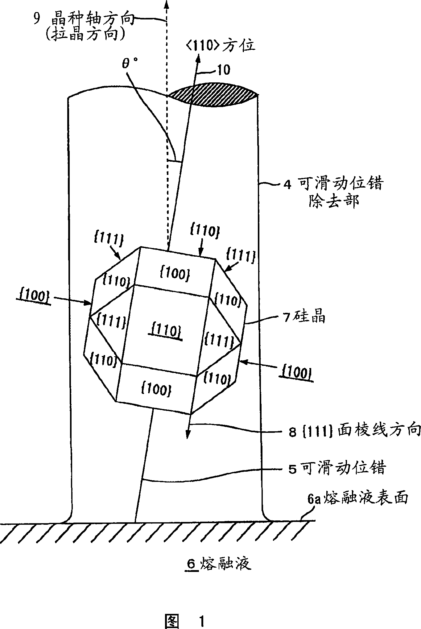
Silicon single crystal manufacturing method and silicon wafer manufacturing method
A manufacturing method and technology of silicon single crystal, applied in the direction of single crystal growth, single crystal growth, chemical instruments and methods, etc., can solve the problems of deterioration of light haze on the surface of epitaxial layer, insufficient dislocation removal effect, etc.
- Summary
- Abstract
- Description
- Claims
- Application Information
AI Technical Summary
Problems solved by technology
Method used
Image

Examples
Embodiment 1
[0079]A silicon single crystal was grown under the crystal growth conditions shown below, and the presence or absence of dislocations in the single crystal was examined. It should be noted that the number of pulled silicon single crystals was three regardless of the boron concentration in the silicon crystal or any level of the inclination angle of the seed crystal.
[0080] The boron concentration of the silicon seed is notated for convenience. "+" or "++" attached to p indicates that the dopant concentration (here, boron concentration) is high and the resistivity of the crystal is low, and "-" indicates the opposite meaning. Since there is no clear definition of dopant concentration and resistivity, P+ and P++ with increased dopant concentration are specifically defined as follows.
[0081] p+: Boron concentration 5×10 17 ~7×10 18 atom / cm 3
[0082] Resistivity 100~20mΩcm
[0083] p++: Boron concentration 7×10 18 ~2×10 20 atom / cm 3
[0084] Resistivity 20~0.8mΩcm ...
Embodiment 2
[0099] A silicon single crystal was grown under the same conditions as in Example 1 except that the neck length was changed to 400 mm. Table 6 shows the results of studies on the presence or absence of dislocations in silicon single crystals.
[0100] Table 6
[0101] Seed Tilt Angle
[0102] As shown in Table 6, by increasing the neck length, dislocation-free can be achieved even under the condition that dislocation-free can not be achieved at a neck length of 300 mm.
Embodiment 3
[0104] A single crystal was grown under the same conditions as in Example 1 except that the neck length was changed to 600 mm. The results of the study are shown in Table 7.
[0105] Table 7
[0106] Seed Tilt Angle
[0107] As can be seen from Table 7, by increasing the neck length, dislocation-free can be achieved even under conditions where dislocation-free can not be achieved in Examples 1 and 2. Examples 2 and 3 are characterized in that the growth of p+ crystals increases the success rate of dislocation-free growth by increasing the neck length. On the other hand, in the growth of p++ crystals, even if the neck length is increased, no dislocations are observed. The success rate of dislocations is improved. It can be seen that the higher the dopant concentration of the silicon melt, the smaller the improvement effect brought about by adjusting the inclination angle of the seed crystal.
PUM
| Property | Measurement | Unit |
|---|---|---|
| diameter | aaaaa | aaaaa |
| diameter | aaaaa | aaaaa |
Abstract
Description
Claims
Application Information