Photo-etching machine imaging quality measuring method
A technology of imaging quality and measurement method, which is applied in the field of measuring the axial image quality parameters of lithography machine by using FOCAL marks with double fine structure, can solve the problem that the measurement range and measurement accuracy cannot be taken into account at the same time, and achieve the reduction of measurement time and high test efficiency. The effect of precision
- Summary
- Abstract
- Description
- Claims
- Application Information
AI Technical Summary
Problems solved by technology
Method used
Image
Examples
Embodiment 1
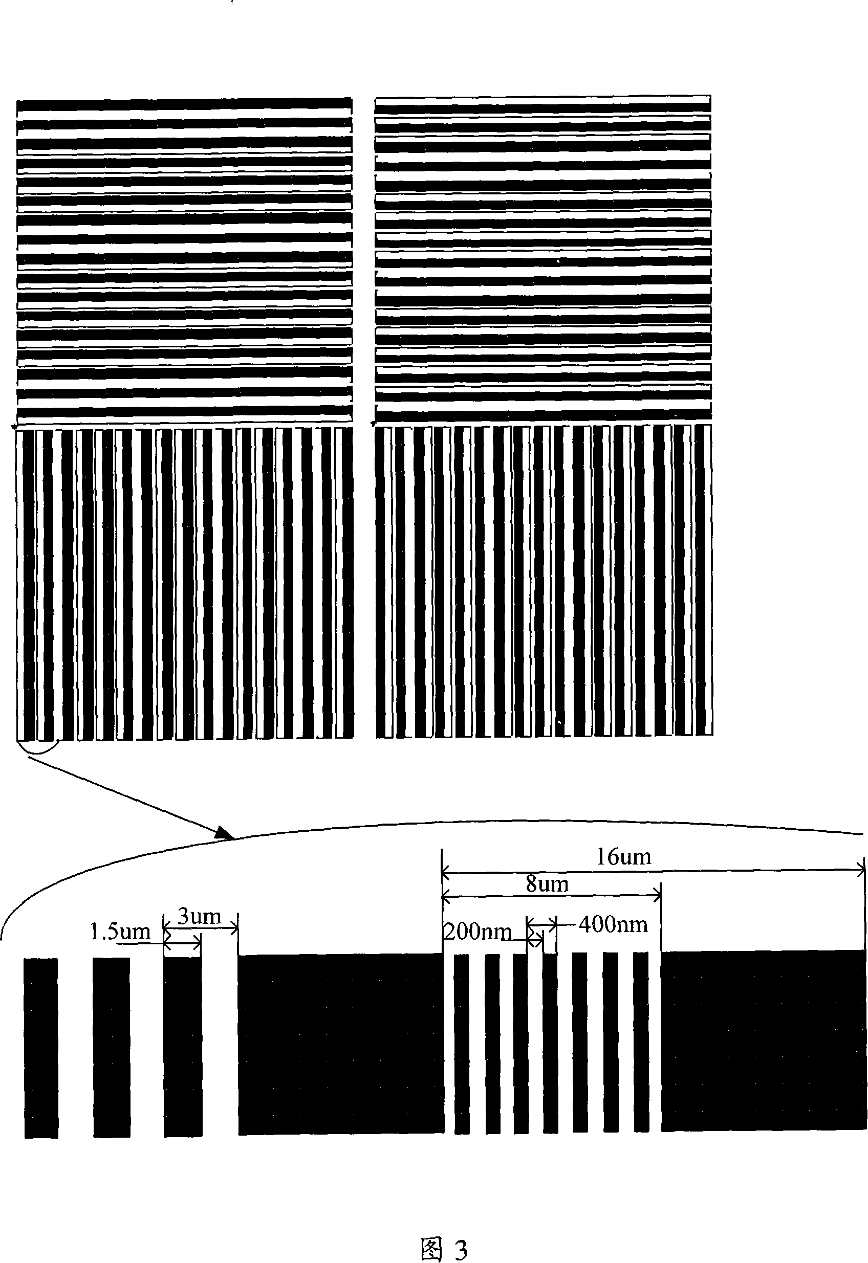
[0036] In this embodiment, the DFOCAL mark as shown in Figure 3 is used, the DFOCAL mark includes an outer layer fine structure and an inner layer fine structure; the line width of the outer layer fine structure is 1.5um, and the line width of the inner layer fine structure is 200nm .
[0037] The steps of the method for measuring the imaging quality of the lithography machine of the present invention are as follows:
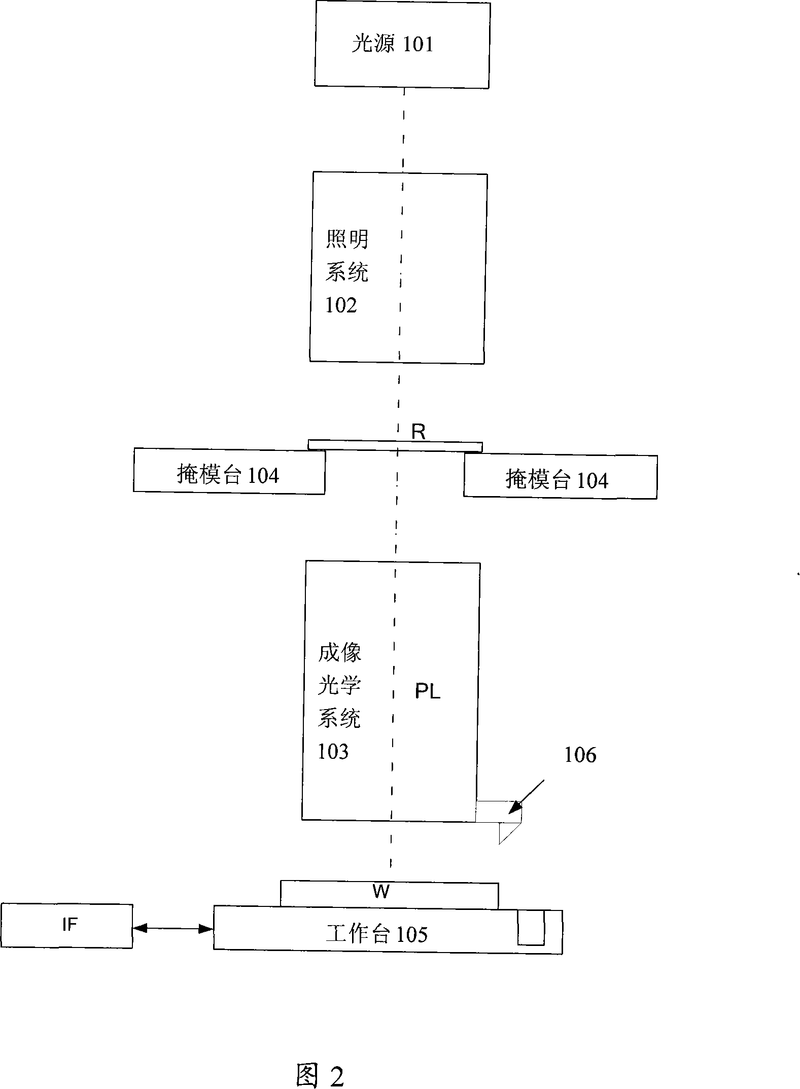
[0038] Step 1. The deep ultraviolet laser emitted by the light source 101 is irradiated by the illumination system 102 onto the mask R engraved with DFOCAL marks, and 65 DFOCAL marks are evenly distributed on the mask R, and the mask R selectively transmits a part of the light. Part of the light passes through the imaging optical system 103, and the pattern on the mask R is exposed and imaged to different parts of the silicon wafer W under 60 defocuss in the range of 3um. As shown in Figure 4, 12 exposures in this range field, each exposure field is divided int...
Embodiment 2
[0049] In this embodiment, the DFOCAL mark as shown in Figure 8 is adopted, and the DFOCAL mark includes an outer layer fine structure and an inner layer fine structure; the line width of the outer layer fine structure is 1.2um, and the line width of the inner layer fine structure is 150nm .
[0050] The steps of the method for measuring the imaging quality of a lithography machine in the present invention are the same as those in Embodiment 1, the only difference being that in Step 1, in this embodiment, the mask pattern is exposed and imaged on the silicon wafer W at 40 defocuss in the range of 2um. on different parts.
[0051] At the same time, the specific calculation method for the relationship between the DFOCAL marker imaging duty cycle and the defocus amount in this embodiment is: CD / 300nm+CD / 2400nm for 150nm line imaging+1200nm line imaging CD / 2400nm, and the specific calculation results are shown in Figure 9 .
[0052] Based on the above, according to different tes...
PUM
 Abstract
Description
Claims
Application Information


