Junction field effect tube and method of manufacturing the same

A field effect transistor and a manufacturing method technology, applied in the field of junction field effect transistor and its manufacturing, can solve problems such as voltage resistance deterioration, and achieve the effects of low cost, increased area, and reduced impurity concentration difference

Inactive Publication Date: 2008-04-30
SANYO ELECTRIC CO LTD +1
View PDF1 Cites 9 Cited by
  • Summary
  • Abstract
  • Description
  • Claims
  • Application Information

AI Technical Summary

Problems solved by technology

[0019] However, in the conventional structure, when the impurity concentration of the channel region 24 is increased, there is a problem that the withstand voltage deteriorates.

Method used


Image

  • Junction field effect tube and method of manufacturing the same
  • Junction field effect tube and method of manufacturing the same
  • Junction field effect tube and method of manufacturing the same

Examples


Embodiment Construction

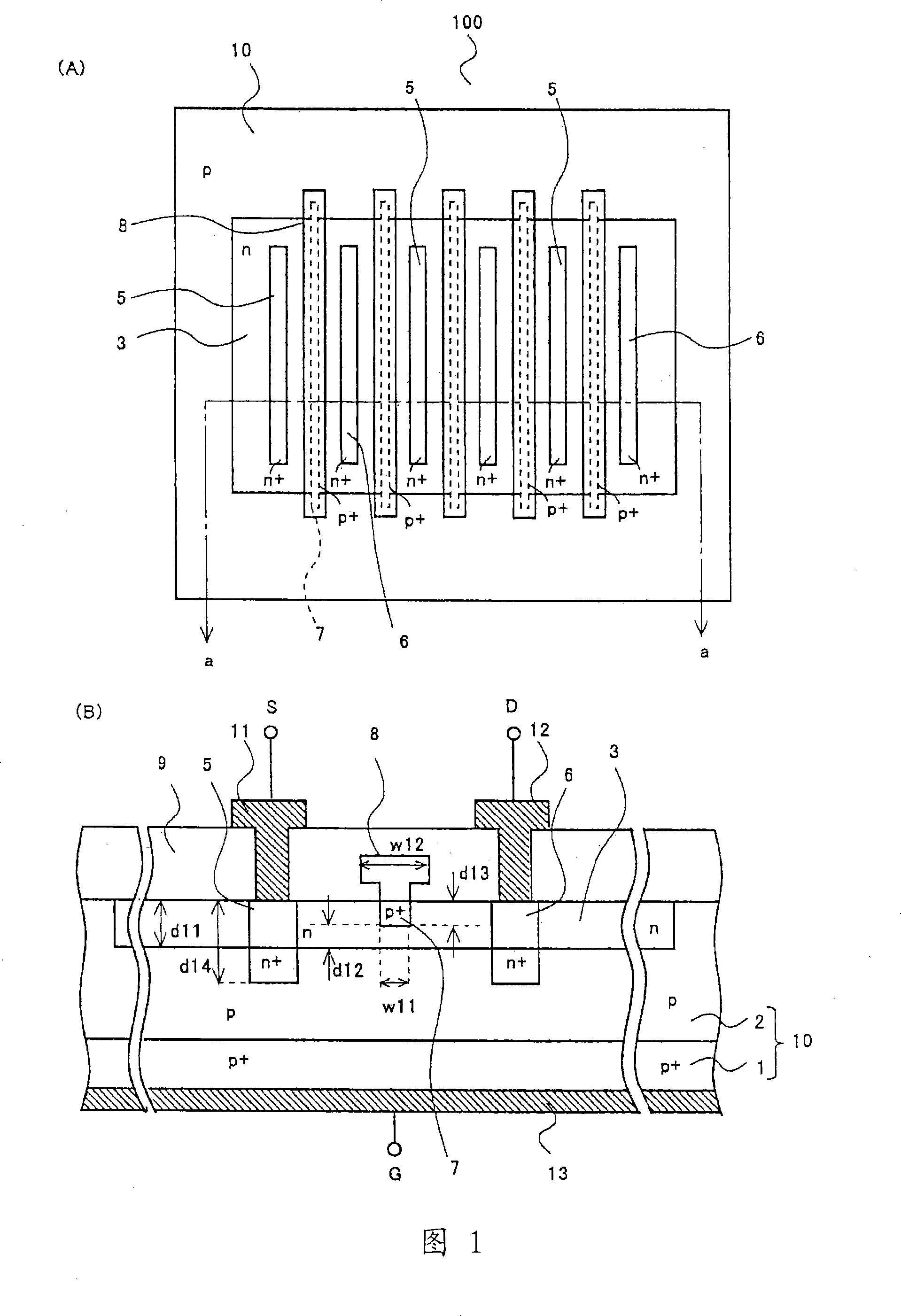
[0073] The junction field effect transistor of the present invention will be described in detail with reference to FIGS. 1 to 8 .

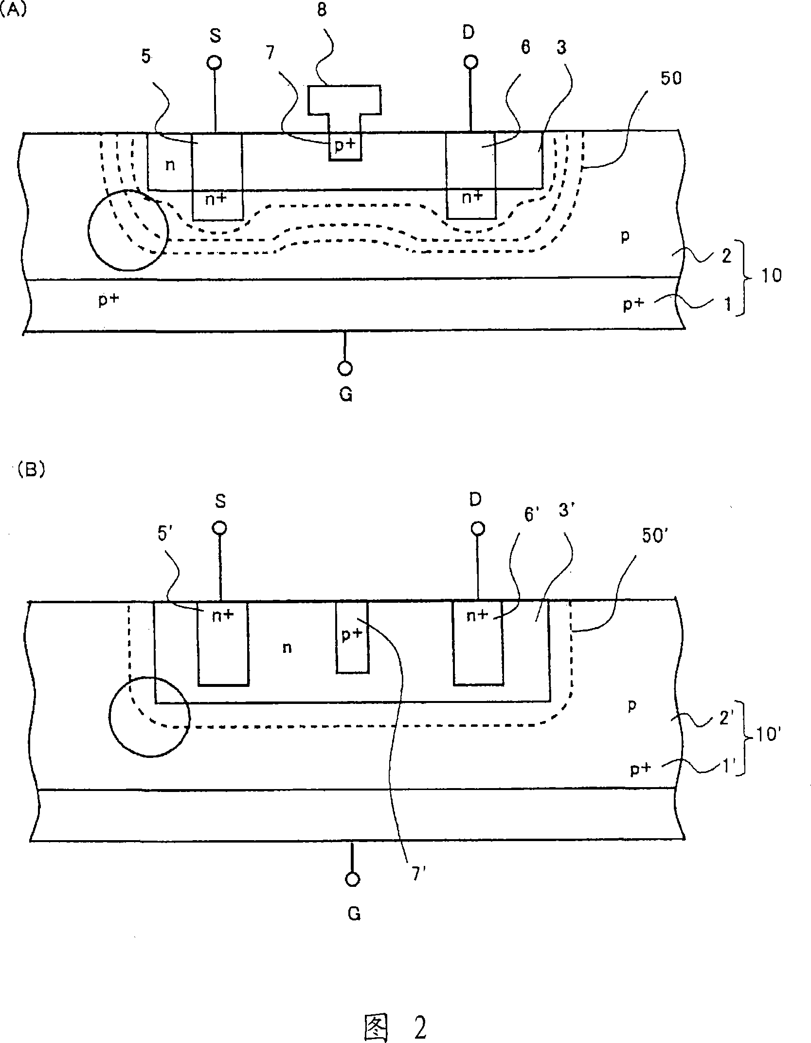
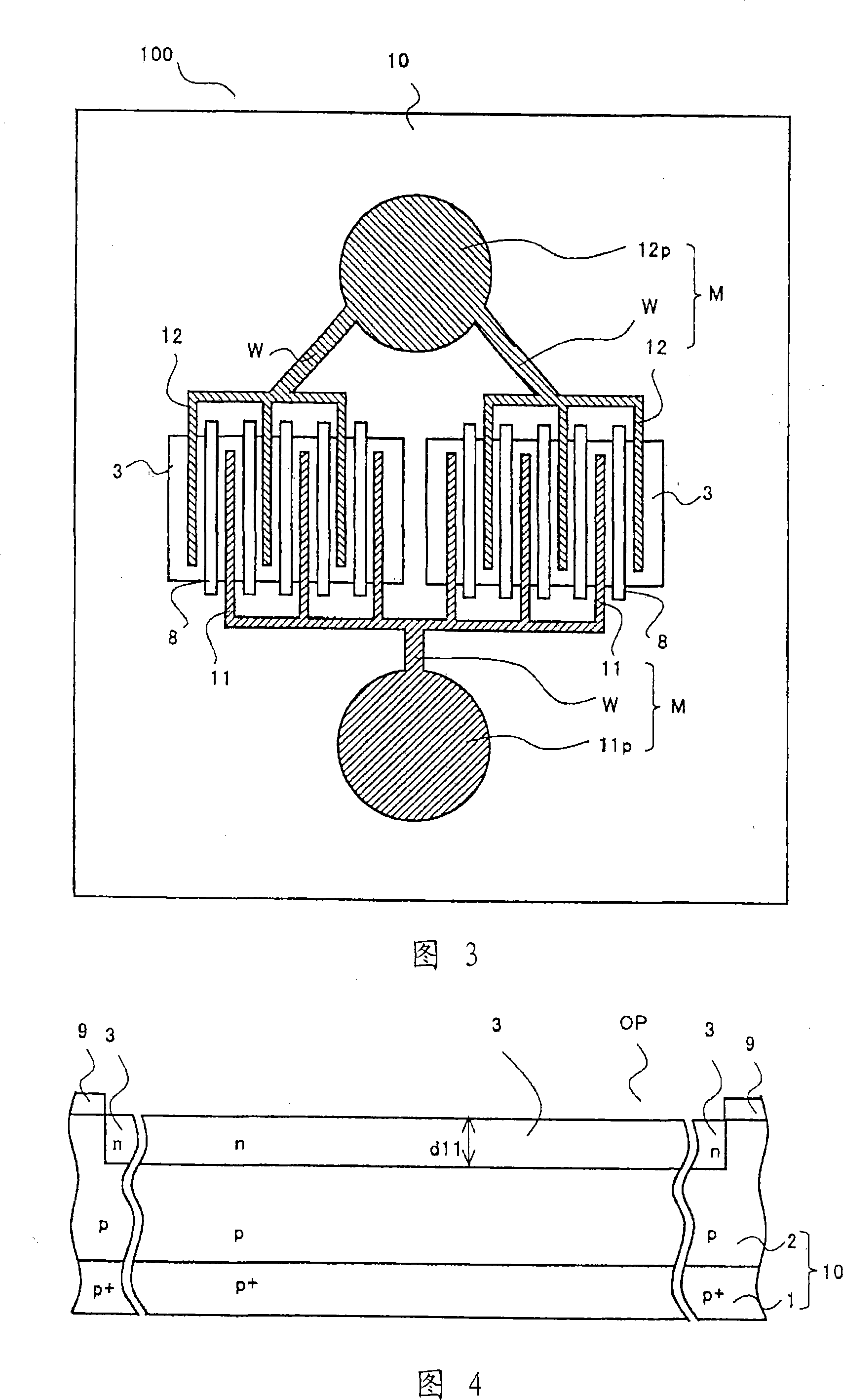
[0074] FIG. 1 is a diagram showing a junction field effect transistor 100 of this embodiment. FIG. 1(A) is a plan view, and FIG. 1(B) is a partial sectional view taken along line a-a of FIG. 1(A). In addition, in FIG. 1(A), the insulating film and metal electrodes (source electrode and drain electrode) on the surface of the substrate are omitted. In addition, FIG. 1(B) shows one cell represented by a set of source region, drain region, and gate region.

[0075] The junction field effect transistor 100 of the present invention is composed of a semiconductor substrate 1 , a semiconductor layer 2 , a channel region 3 , a source region 5 , a drain region 6 , a gate region 7 , and a conductive layer 8 .

[0076] Referring to FIG. 1(A), an n-type channel region 3 is provided on the surface of a p-type semiconductor substrate 10 . On the surface of th...


PUM


Abstract

A shallow channel region is selectively formed by ion implantation and diffusion. Since the channel region forms pn junctions with a p type semiconductor layer having a relatively low impurity concentration, a reduction of a junction capacitance leads to improvement in high-frequency characteristics. Moreover, since a gate region can also be shallowly formed by ion implantation, noise can be reduced by reduction in an internal resistance. Furthermore, a breakdown voltage and electrostatic breakdown characteristics can be improved by allowing the source and drain regions to penetrate the channel region.

Description

technical field [0001] The invention relates to a junction field effect transistor (FET) and a manufacturing method thereof, in particular to a junction field effect transistor with high withstand voltage and capable of improving high-frequency characteristics and noise characteristics and a manufacturing method thereof. Background technique [0002] In the existing junction field effect transistor, for example, an n-type trap region used as a channel region is provided on a p-type semiconductor substrate, an n+ type source region and a drain region are arranged in the n-type trap region, and an n+ type source region and a drain region are arranged in the source region. A gate region is formed between the drain region and the drain region (for example, refer to Patent Document 1). [0003] A conventional junction field effect transistor 200 will be described with reference to FIG. 9 . FIG. 9(A) is a plan view showing a conventional junction field effect transistor 200, and ...

Claims


Application Information

Patent Timeline
Patent Type & Authority Applications(China)
IPC IPC(8): H01L29/808H01L21/337
CPCH01L29/808H01L29/66901H01L29/1066
Inventor 小林俊介
Owner SANYO ELECTRIC CO LTD
Why Eureka
Try Eureka