Image sensor structure and manufacturing method thereof

A technology of an image sensor and a manufacturing method, which is applied in the manufacturing of semiconductor/solid-state devices, radiation control devices, electrical components, etc., can solve the problems of increased density of pixel area image sensors, deterioration of crosstalk phenomenon, etc.

Inactive Publication Date: 2008-05-07
POWERCHIP SEMICON CORP
View PDF0 Cites 6 Cited by
  • Summary
  • Abstract
  • Description
  • Claims
  • Application Information

AI Technical Summary

Problems solved by technology

As the degree of integration increases, the pixel area shrinks and the density of the entire image sensor increases due to the use of a multi-layer dielectric layer structure, which worsens the crosstalk phenomenon

Method used


Image

  • Image sensor structure and manufacturing method thereof
  • Image sensor structure and manufacturing method thereof
  • Image sensor structure and manufacturing method thereof

Examples


Embodiment Construction

[0030] The image sensor of the preferred embodiment of the present invention and the method for forming it are described in more detail below using process cross-sectional diagrams. In each embodiment of the present invention, the same symbols represent the same components.

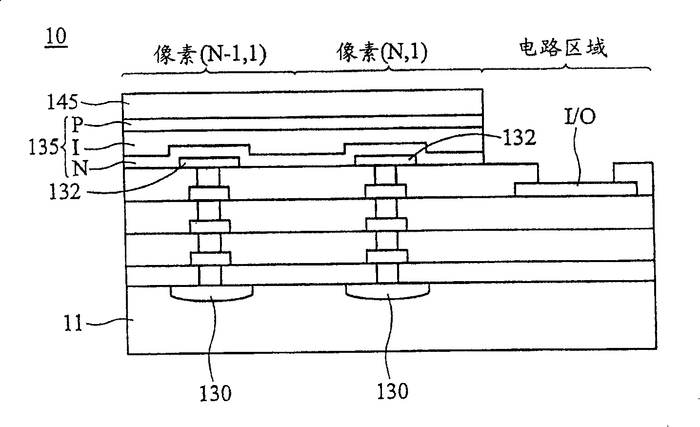
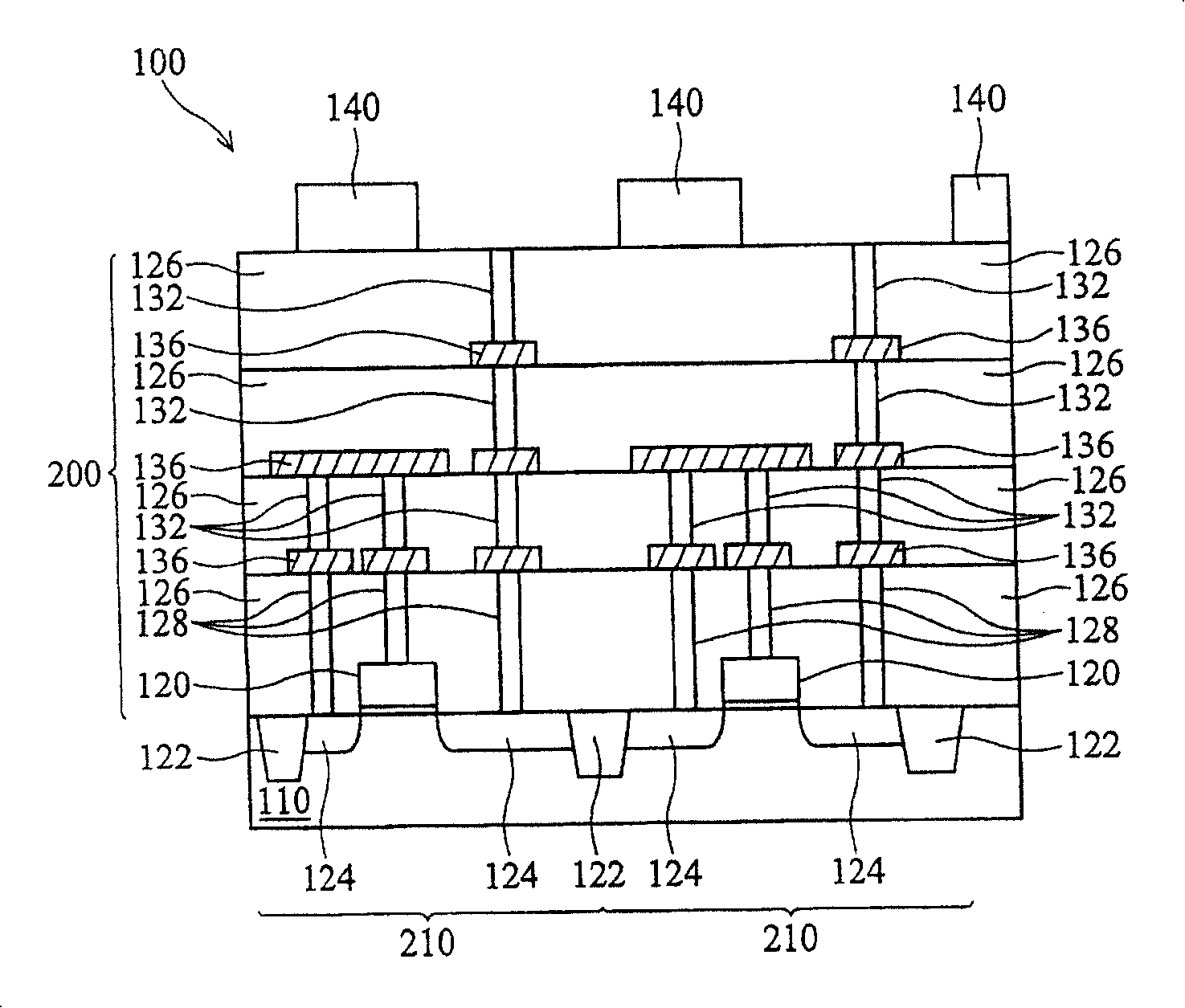
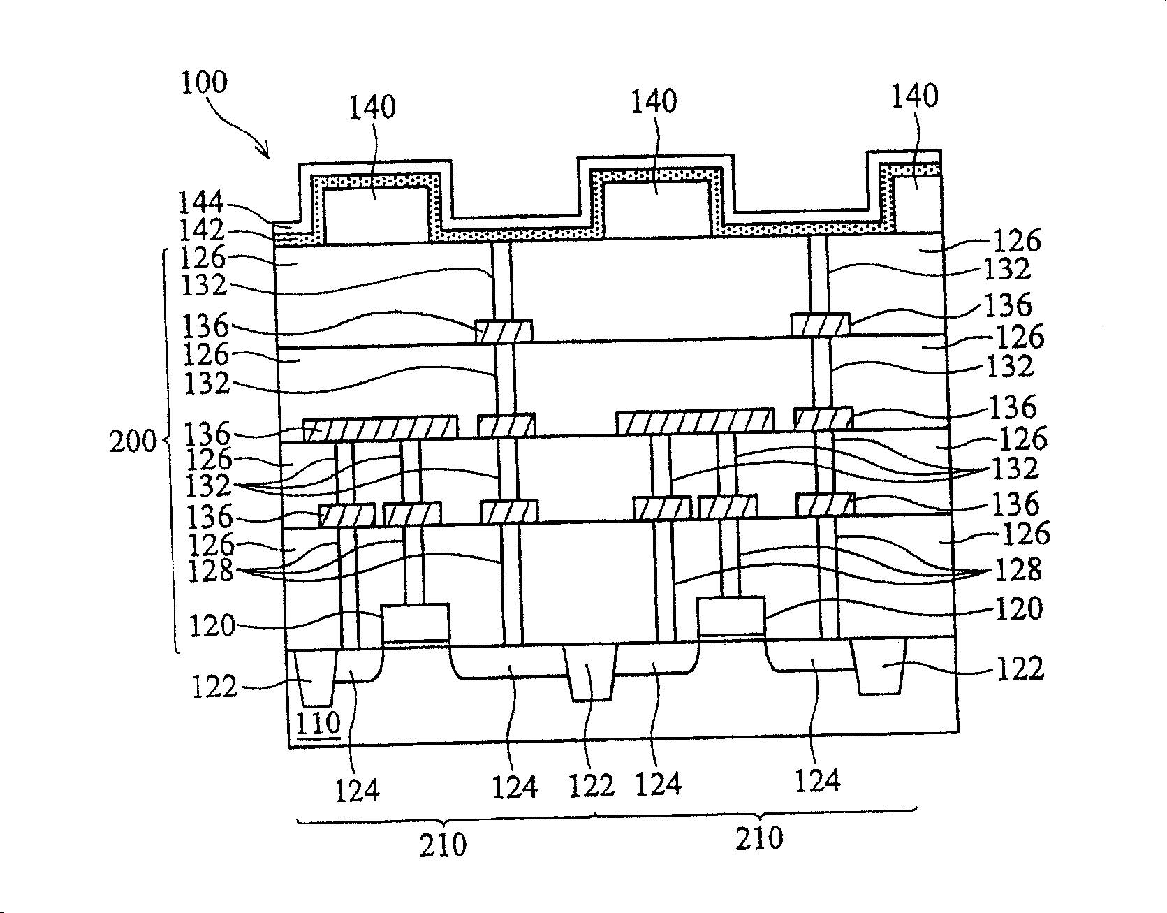
[0031] Please refer to Figures 2a to 2f , which shows a series of cross-sectional process diagrams of the image sensor structure 100 according to the preferred embodiment of the present invention. Please refer to FIG. 2a, the main components forming the image sensor structure 100 of the preferred embodiment of the present invention include a substrate 110, which includes a plurality of pixel regions 210, and the substrate 110 can be a silicon substrate, a silicon on insulator (silicon on insulator, SOI) substrate or other semiconductor material substrates. A plurality of shallow trench isolations (shallow trench isolation, STI) 122 are formed in the substrate 110 . One or more image sensor circuit stru...


PUM


Abstract

The invention provides a manufacturing method of an image sensor structure, comprising a substrate, an image sensor circuit structure on the substrate, a patterned stopping layer on the image sensor circuit structure; in turn, on the patterned stopping layer and the image sensor circuit structure uncovered by the patterned stopping layer lie in order a first doped amorphous silicon layer, a first undoped amorphous silicon layer. Planarization steps are carried to remove partial first undoped amorphous silicon layer, the first doped amorphous silicon layer, the electrode layer and the patterned stopping layer; thus the remained electrode layer, the first doped amorphous silicon layer and the first undoped amorphous silicon layer are separated by the patterned stopping layer.

Description

technical field [0001] The present invention relates to a method for manufacturing an image sensor structure, in particular to a method for manufacturing a photodiode layer (Photoconductor on active pixel, POAP) type image sensor. Background technique [0002] Photoconductor on active pixel (POAP) type image sensor (image sensor) (hereinafter referred to as POAP type image sensor) has been widely used in many application fields, such as digital camera (digital camera), digital video camera ( digital video camera), monitor (monitor), mobile phone (mobile phone), etc. The POAP image sensor mainly uses a photoconductor (Photoconductor) covered on an active pixel array or an image sensor cell array, which includes a photodiode (Photodiode) to convert incident image light energy into digital data. [0003] The POAP image sensor can sense light of different wavelengths such as visible light, X-ray (X-ray), ultraviolet light (ultraviolet, UV), infrared light (infrared ray, IR), a...

Claims


Application Information

Patent Timeline
Patent Type & Authority Applications(China)
IPC IPC(8): H01L21/822H01L27/146
Inventor 陈宥先黄明山汪嘉将
Owner POWERCHIP SEMICON CORP
Why Eureka
Try Eureka