

Non-volatile organic thin-film transistor memory based on floating gate structure and manufacturing method therefor
A non-volatile, organic thin-film technology, applied in semiconductor/solid-state device manufacturing, electrical solid-state devices, semiconductor devices, etc., to reduce the chance of contamination, improve device performance, and good storage performance
- Summary
- Abstract
- Description
- Claims
- Application Information
AI Technical Summary
Problems solved by technology
Method used
Image

Examples
Embodiment 1
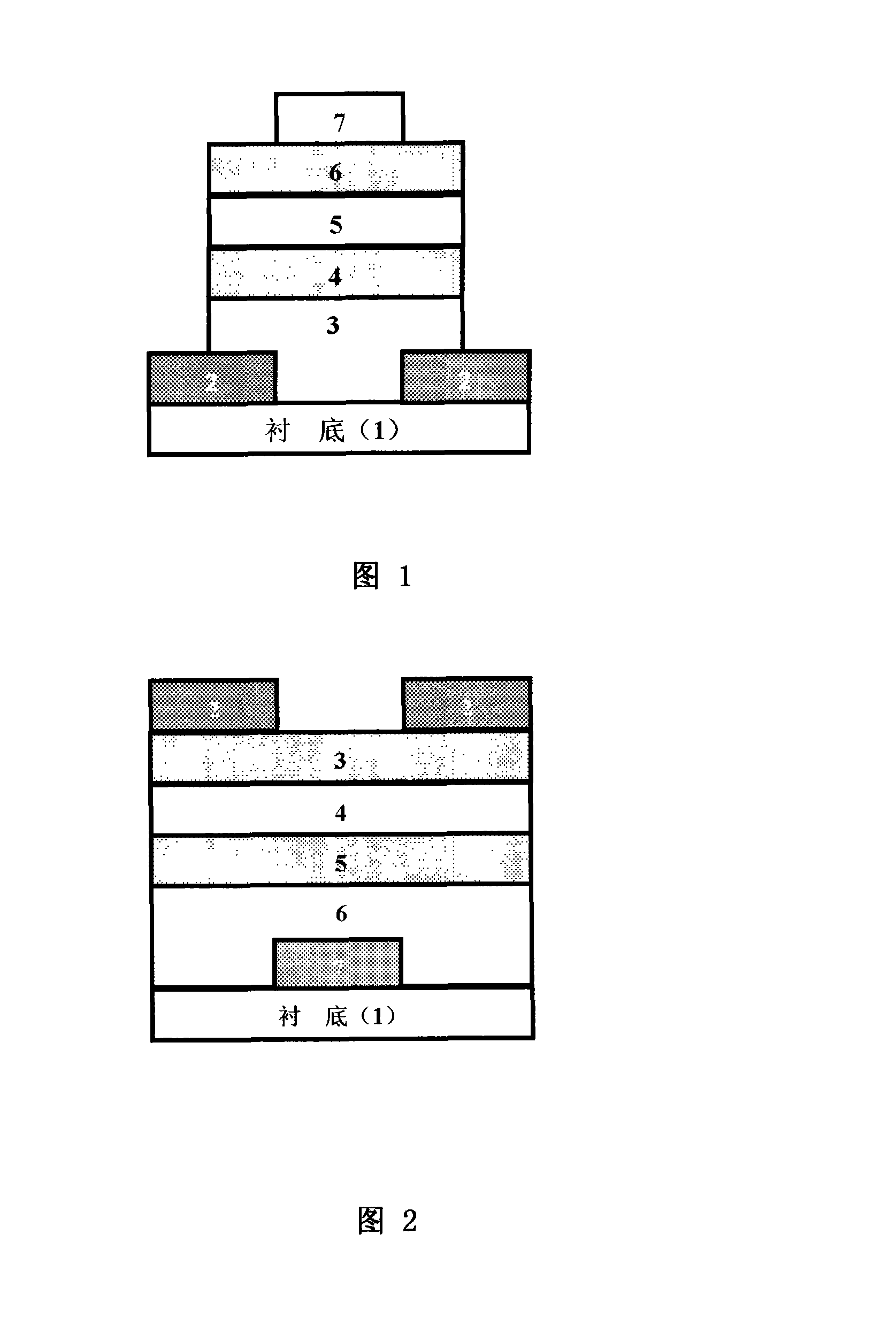
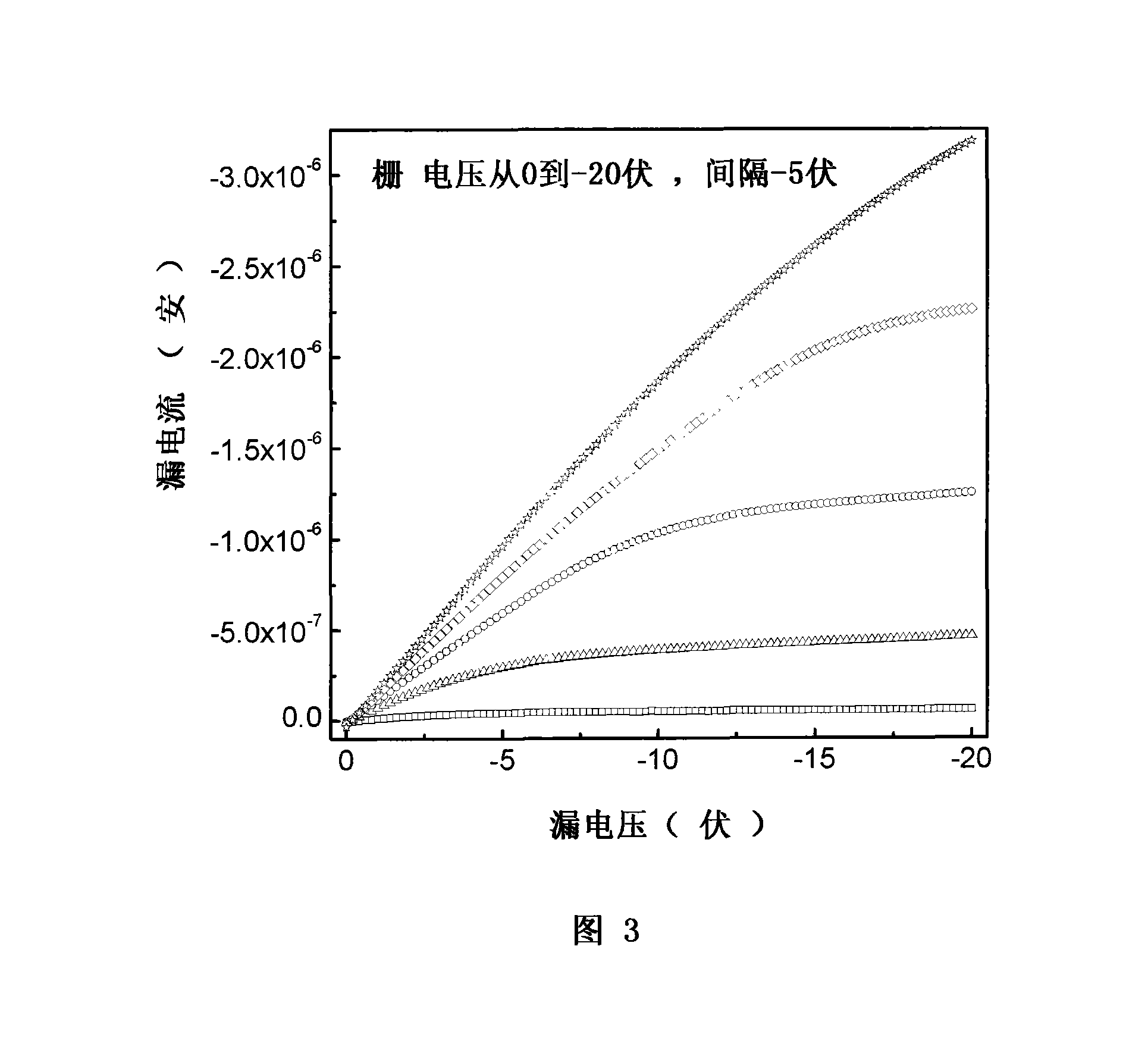
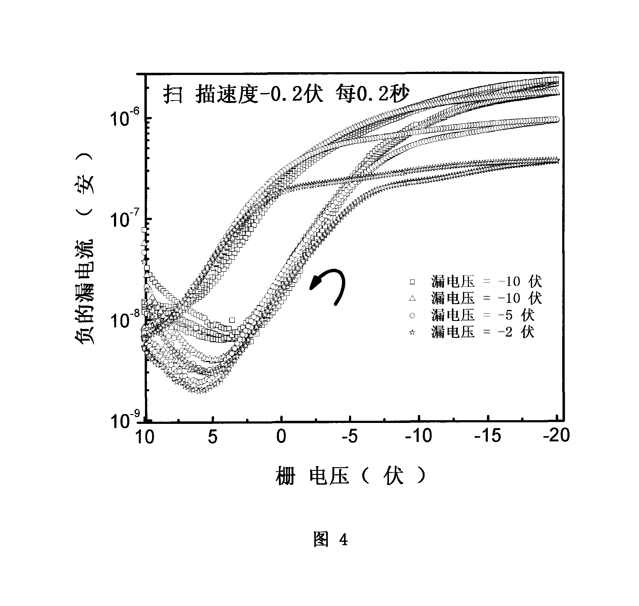
[0052] First, the indium tin oxide on the indium tin oxide glass is photoetched into two electrodes (ie, source and drain electrodes) with a length of 10 mm and a width of 1 mm (ie, the channel width), and the distance between the electrodes is 20 microns (ie, the channel length ); then cleaned and blown dry with nitrogen. In a vacuum of 1 to 5 x 10 -4 In PA’s coating system, 70nm-thick pentacene, 25nm-thick nylon 6, 8nm-thick nickel, 200nm-thick nylon 6, and 150nm-thick special Fulong, and patterned through a mask, and finally a 100nm thick strip of aluminum with a width of 1 mm, patterned through another mask. The growth rate of pentacene film is controlled at 0.05 nanometers per second, the growth rate of nickel film is controlled at 0.02 nanometers per second, and the growth rate of nylon 6 and Teflon is controlled at 0.1 nanometers per second. Figure 3 shows the output characteristic curves of the organic thin film transistor storage device based on the floating gate st...
Embodiment 2
[0054] First, the indium tin oxide on the indium tin oxide glass is photolithographically formed into two electrodes (ie, source and drain electrodes) with a length of 10 mm and a width of 1 mm (ie, the channel width), and the distance between the electrodes is 100 microns (ie, the channel length ); then cleaned and blown dry with nitrogen. In a vacuum of 1 to 5 x 10 -4 In PA’s coating system, 70nm-thick pentacene, 25nm-thick nylon 6, 15nm-thick calcium fluoride, 200nm-thick nylon 6, 150nm-thick Teflon and patterned through a mask, and finally aluminum strips 100 nm thick and 1 mm wide, patterned through another mask. The growth rate of pentacene film is controlled at 0.05 nanometers per second, the growth rate of calcium fluoride film is controlled at 0.05 nanometers per second, and the growth rate of nylon 6 and Teflon is controlled at 0.1 nanometers per second. The device has obvious field effect characteristics, and the operating voltage of the device can be reduced to w...
Embodiment 3
[0056] First, the indium tin oxide on the indium tin oxide glass is photoetched into two electrodes (ie, source and drain electrodes) with a length of 10 mm and a width of 50 microns (ie, the channel width), and the distance between the electrodes is 1 micron (ie, the channel length ); then cleaned and blown dry with nitrogen. In a vacuum of 1 to 5 x 10 -4 In PA’s coating system, 50nm-thick pentacene, 2nm-thick Teflon, 2nm-thick nickel, and 100nm-thick Teflon are sequentially deposited on the source and drain electrodes of indium tin oxide, and the The stencil was patterned and finally the 80nm thick strip of aluminum with a width of 1mm was patterned through another mask. The growth rate of pentacene film is controlled at 0.05 nanometers per second, the growth rate of nickel film is controlled at 0.02 nanometers per second, and the growth rate of Teflon is controlled at 0.1 nanometers per second. The device has obvious field effect characteristics, and the operating voltage...
PUM
 Abstract
Description
Claims
Application Information