High temperature resistant high photics reflexive conductive film and preparation method thereof

A technology of optical reflection and conductive film, applied in chemical instruments and methods, optics, optical components, etc., can solve the problems of structural damage, agglomeration and agglomeration, conduction failure of silver film, and achieve high optical reflection performance and good electrical conductivity. , Overcome the effects of agglomeration and agglomeration

Inactive Publication Date: 2008-05-28
FUJIAN NORMAL UNIV
View PDF0 Cites 23 Cited by
  • Summary
  • Abstract
  • Description
  • Claims
  • Application Information

AI Technical Summary

Problems solved by technology

However, the silver thin film is prone to agglomeration and agglomeration under high temperature conditions, which causes the structure of the silver thin film to be destroyed, the conduction fails, and the optical reflection performance decreases.
That is to say, pure silver films cannot achieve high optical reflection and good electrical conductivity under high temperature conditions.

Method used


Image

  • High temperature resistant high photics reflexive conductive film and preparation method thereof

Examples


Embodiment 1

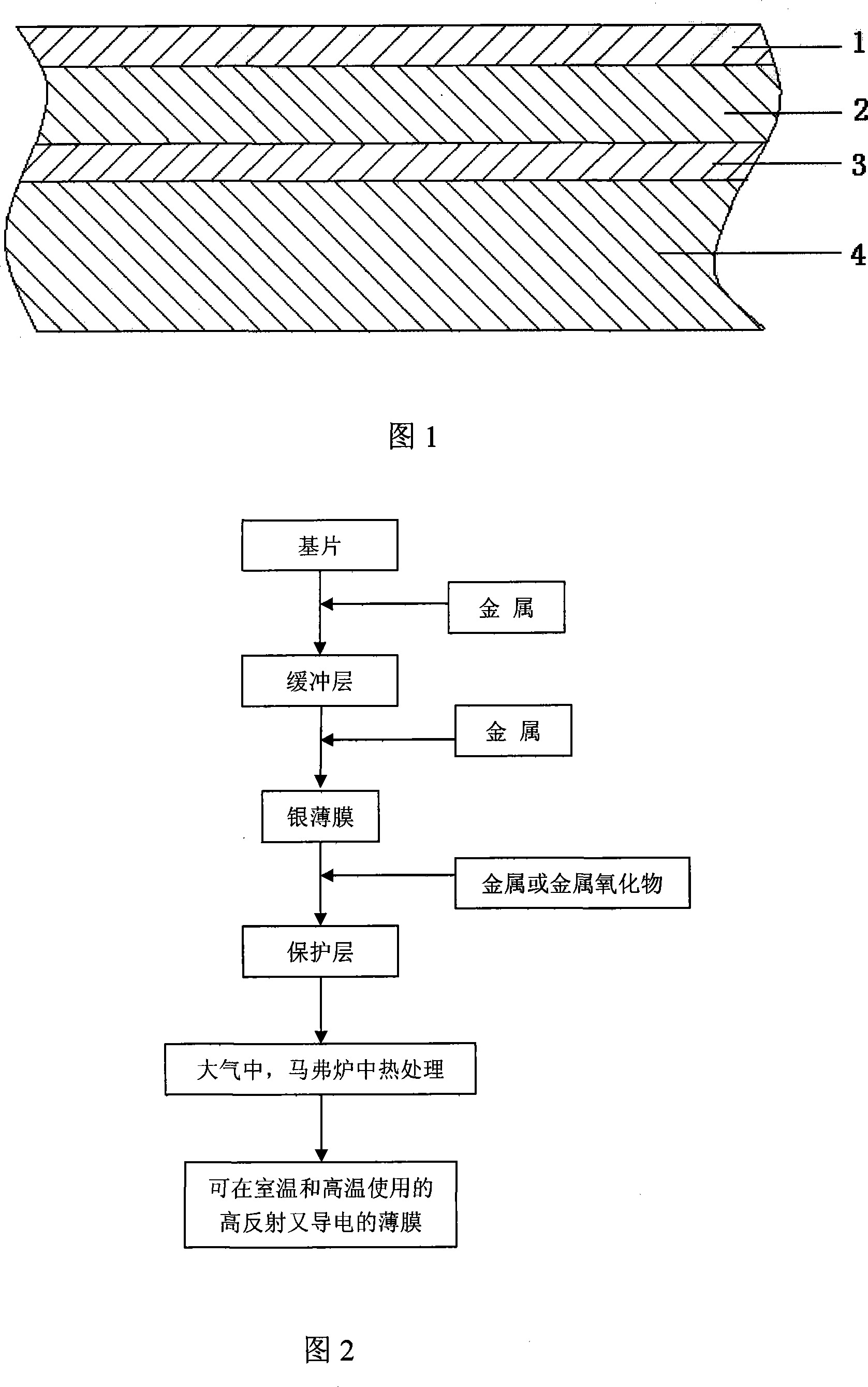
[0028] It includes a base layer 4; a thin film buffer layer 3 arranged on the base layer 4; a thin film conductive layer 2 attached to the buffer layer 3; and a thin film protective layer 1 attached to the thin film conductive layer 2. Wherein: the base layer material is quartz; the buffer layer material is aluminum thin film, the thin film conductive layer material is silver, and the thin film protective layer material is silicon oxide.

[0029] 1. Preparation of thin film buffer layer

[0030] The aluminum thin film was deposited on the quartz substrate by magnetron sputtering, the film thickness was 30 nanometers, the sputtering target material was metal aluminum, the sputtering power was 100 watts, and the sputtering gas pressure was 0.9 Pa.

[0031] 2. Preparation of thin film conductive layer silver

[0032] Using magnetron sputtering to deposit a metallic silver film on the surface deposited with the aluminum film, the thickness of the silver film is 250 nm, the sputte...

Embodiment 2

[0038] It includes a base layer 4 ; a thin film buffer layer 3 arranged on the substrate 4 ; a thin film conductive layer 2 attached to the buffer layer 3 ; Wherein: the base layer material is single crystal silicon wafer; the buffer layer material is aluminum and copper mixed film, the film conductive layer material is silver, and the film protective layer material is zinc oxide film.

[0039] 1. Preparation of thin film buffer layer

[0040] A mixed film of copper and aluminum was deposited on a single crystal silicon substrate by magnetron sputtering. The thickness of the film was 30 nanometers. The sputtering target material was a mixture of metal copper and aluminum. The weight ratio of copper and aluminum was 1:1. The power was 100 watts, and the sputtering gas pressure was 0.9 Pa.

[0041] 2. Preparation of thin film conductive layer silver

[0042] Using magnetron sputtering to deposit a metal silver film on the surface deposited with copper and aluminum mixed film, ...


PUM

PropertyMeasurementUnit
thicknessaaaaaaaaaa
thicknessaaaaaaaaaa
thicknessaaaaaaaaaa

Abstract

The invention relates to a conductive film with high optical reflection, which can be used in the atmosphere environmental with the temperature ranging from room temperature to 550 DEG C, and a preparation method of the conductive film. The conductive film provided by the invention comprises a basic piece, a film damping layer, a film conductive layer, a film protection layer, all of which are arranged layer by layer from bottom to top. The conductive layer is metal silver film with the thickness ranging from 150 nm to 300 nm; the lower surface of the conductive layer is the film damping layer with the thickness ranging from 10 nm to 40nm; the upper surface of the film conductive layer is a film protection layer with the thickness ranging from 5nm to 15nm. The preparation method is that plating technology is adopted; the damping layer, the conductive layer and the protection layer are sequentially plated on the basic piece layer, and finally the heat disposal is carried out by virtue of a muffle. By taking metal and metal oxide as the damping layer and the protection layer of the silver film, the invention can effectively restrict the agglomeration and coacervation of the silver film under high temperature, and implements that the prepared film can remain excellent conductive performance and high optical reflection performance under high temperature.

Description

technical field [0001] The invention relates to a conductive film and a preparation method thereof, in particular to a conductive film with high optical reflection and can be used in an atmospheric environment ranging from room temperature to 550° C. and a preparation method thereof. Background technique [0002] Films have been widely used in defense, communications, aviation, aerospace and industrial and agricultural production. Optical high-reflection films are usually used for civilian mirrors, aluminized films in parabolic solar receivers in solar cookers, coated mirrors in large-scale astronomical instruments and precision optical instruments, high-reflection films for various lasers, etc. Good conductive films (such as Al, Cu, Cr, Pt, Au, Ag films, etc.) are commonly used in semiconductor devices and integrated circuits. With the advancement of science and technology, special requirements have also been placed on the properties of thin films. For example, for GaN-bas...

Claims


Application Information

Patent Timeline
Patent Type & Authority Applications(China)
IPC IPC(8): B32B15/04B32B9/00C23C14/56C23C14/58H01B5/00H01B13/00G02B1/00
Inventor 赖发春吕晶黄志高林丽梅吴小春
Owner FUJIAN NORMAL UNIV
Why Eureka
Try Eureka