Inductance measuring encapsulation part and its making method

A manufacturing method and packaging technology, which are used in semiconductor/solid-state device manufacturing, electrical components, electrical solid-state devices, etc., can solve the problems of size limitation, intrusion, cracking and other problems of sensing packages, so as to avoid affecting product life, The effect of enhancing adhesion

Inactive Publication Date: 2008-05-28
SILICONWARE PRECISION IND CO LTD
View PDF4 Cites 7 Cited by
  • Summary
  • Abstract
  • Description
  • Claims
  • Application Information

AI Technical Summary

Problems solved by technology

[0005] However, in the aforementioned sensing package, since the glass 15 and the sensing chip 10 are joined by the adhesive layer 14 and part of the encapsulation material 16, it is often caused by poor adhesion when the temperature of the use environment changes. A crack C occurs at the joint between the side of the glass 15 and the packaging material 16, such as Figure 1B As shown, it may even lead to the intrusion of external water vapor or pollutants into the sensing chip 10, which seriously affects the life of the product.
[0006] Therefore, how to provide a sensing package and its manufacturing method can avoid being limited by the chip carrier and at least reserve enough space to place the dam structure, so that the size of the sensing package is limited, At the same time, due to the poor adhesion of the light-transmitting glass and the packaging material, cracks occur, and even external moisture or pollutants intrude into the package, etc., which is indeed an urgent issue in related fields.

Method used


Image

  • Inductance measuring encapsulation part and its making method
  • Inductance measuring encapsulation part and its making method
  • Inductance measuring encapsulation part and its making method

Examples


no. 1 example

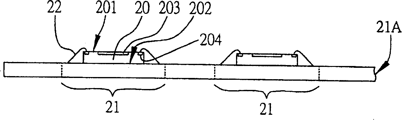
[0085] see Figure 2A to Figure 2D , is a schematic diagram of the sensing package and its manufacturing method of the present invention, and will be illustrated by mass-manufacturing the sensing package of the present invention in a batch manner.

[0086] Such as Figure 2A As shown, a module sheet 21A with a multi-chip carrier 21 is provided to mount the sensor chip 20 on the chip carrier 21 .

[0087] The sensing chip 20 has an active surface 201 and an opposite non-active surface 202, and the active surface 201 of the sensing chip 20 is provided with a sensing region 203 and an electrode pad 204, and the sensing chip 20 is based on its non-active surface. The active surface 202 is correspondingly placed on the chip carrier 21, and the electrode pads 204 of the sensing chip 20 and the chip carrier 21 are connected by bonding wires 22, so that the sensing chip 20 and the chip carrier 21 are electrically connected to each other. coupling. In addition, the sensing chip 20 c...

no. 2 example

[0093] see Figure 3A to Figure 3D , is a schematic diagram of the second embodiment of the sensing package and its manufacturing method of the present invention. This embodiment is roughly the same as the previous embodiment, the main difference is that in the previous embodiment, in order to allow the light-transmitting body to be connected to the sensing chip through the adhesive layer, a certain distance must be preset between the sensing area of ​​the sensing chip and the electrode pad. The distance (generally greater than 300 μm) will relatively increase the size of the required sensing chip; and in this embodiment, the adhesive layer is mainly heated to make the adhesive layer appear in a molten state, and the bonding wire is directly connected to the end of the sensing chip. After the adhesive layer is cured, the light-transmitting body can cover and seal the sensing area, so as to save the pre-installed light-transmitting body between the sensing area of ​​the sensing...

no. 3 example

[0104] see also Figure 4A and Figure 4B , is a schematic cross-sectional view of the third embodiment of the manufacturing method of the sensing package of the present invention. This embodiment is substantially the same as the previous embodiment, and only the main difference is shown for simplification of the drawings, that is, after the sensing chip 40 is placed and electrically connected on the module sheet 41A with the multi-chip carrier 41, the sensing chip 40 is then placed on the sensing chip 41A. The chip 40 is covered with a monolithic light-transmitting body 45A such as glass, wherein the peripheral dimension of the monolithic light-transmitting body 45A exceeds the cut-off line of the sensing package to be completed, and the monolithic light-transmitting body 45A A plurality of adhesive layers 34 are provided on the body 45A, and the position of the adhesive layer is corresponding to the sensing chip 40 connected to each of the chip carriers 41, and makes it cov...


PUM


Abstract

The invention relates to a sensing encapsulation part and a manufacturing method thereof. A sensing chip is arranged on and communicated to a load bearing part of a chip through a welding line to provide a light transmission body to be connected with the sensing chip with an interval of an adhesive layer, wherein, the size of a starting plane of the light transmission body is larger than the predetermined completion size of the sensing encapsulation part. A glue seal layer is formed on the load bearing part of the chip again to coat the sensing chip and the welding line and expose the upper surface of the light transmission body. Later, the cutting is carried out along the predetermined completion plane size of the sensing encapsulation part, thereby forming the sensing encapsulation part, the size of which is the same with the light transmission body. Furthermore, the contact area of the light transmission body and the glue seal layer is increased to strengthen the conjunction of the light transmission body.

Description

technical field [0001] The invention relates to a semiconductor package and its manufacturing method, in particular to a sensing package and its manufacturing method. Background technique [0002] The traditional image sensor package mainly connects the sensor chip (Sensor chip) on a chip carrier, and electrically connects the sensor chip and the chip carrier through bonding wires, and then A glass is sealed above the sensing chip so that the image light can be obtained by the sensing chip. In this way, the image-sensing package with the completed structure can be installed by the system manufacturer on an external device such as a printed circuit board (PCB), for example, a digital camera (DSC), a digital video camera (DV), an optical mouse, etc. , mobile phones, fingerprint readers and other electronic products. [0003] In the existing sensing packages disclosed in U.S. Patent Nos. 6,060,340, 6,262,479, and 6,590,269, the dam structure is pre-prepared on the chip carrie...

Claims


Application Information

Patent Timeline
Patent Type & Authority Applications(China)
IPC IPC(8): H01L21/50H01L21/60H01L27/146
CPCH01L2224/49175H01L24/97H01L2924/15311H01L2224/48091H01L2224/48227H01L2924/30107H01L2924/16235H01L2924/1815H01L2924/00014H01L2924/00
Inventor 张泽文詹长岳黄致明萧承旭
Owner SILICONWARE PRECISION IND CO LTD
Why Eureka
Try Eureka