Layer sequence and method of manufacturing a layer sequence
A layer sequence, nickel layer technology, applied in the field of manufacturing layer sequence, can solve the problems of time-consuming and expensive, and achieve the effect of simplifying the manufacturing process, reducing the total cost and making the production simple
- Summary
- Abstract
- Description
- Claims
- Application Information
AI Technical Summary
Problems solved by technology
Method used
Image
Examples
Embodiment Construction
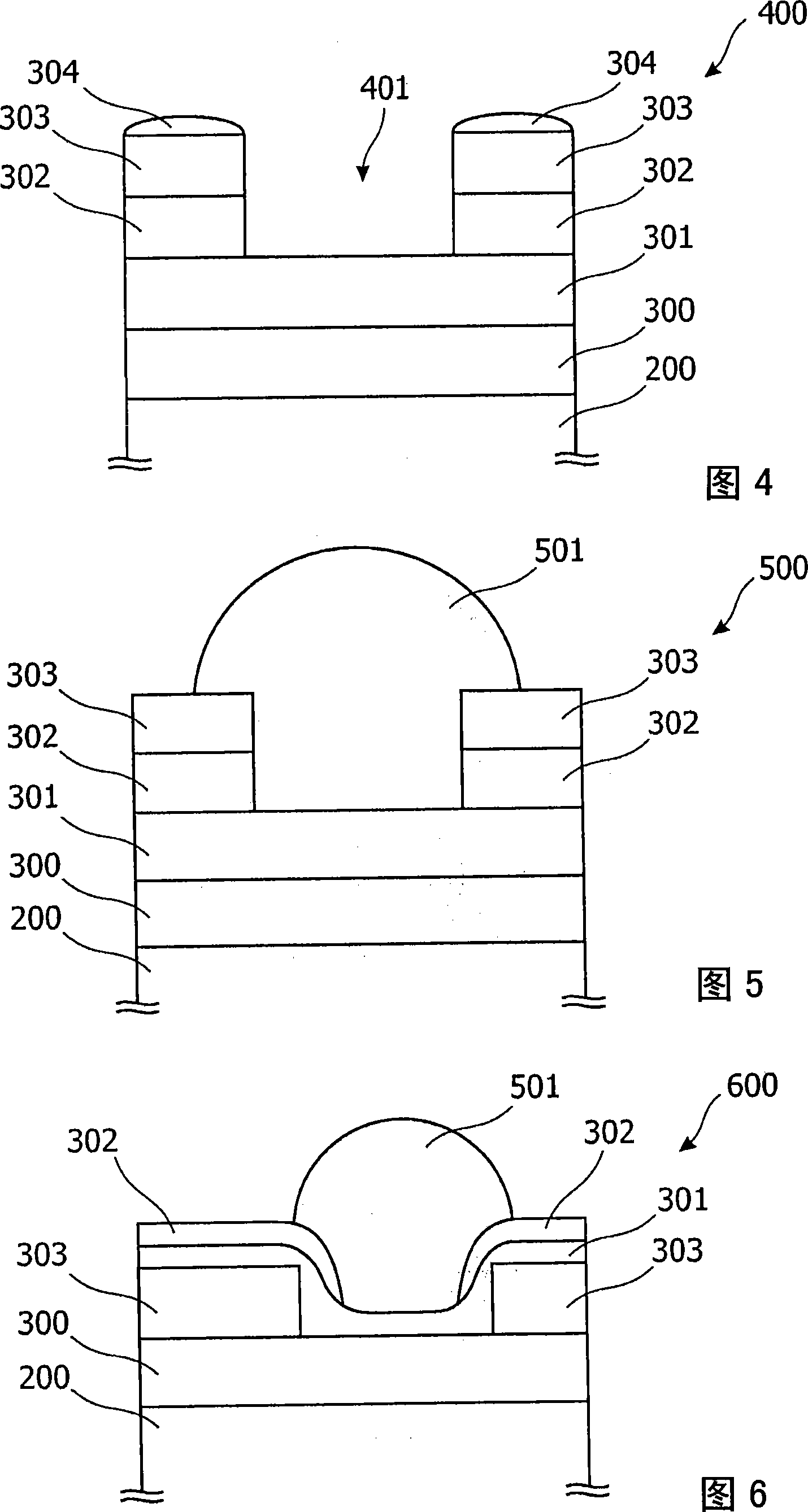
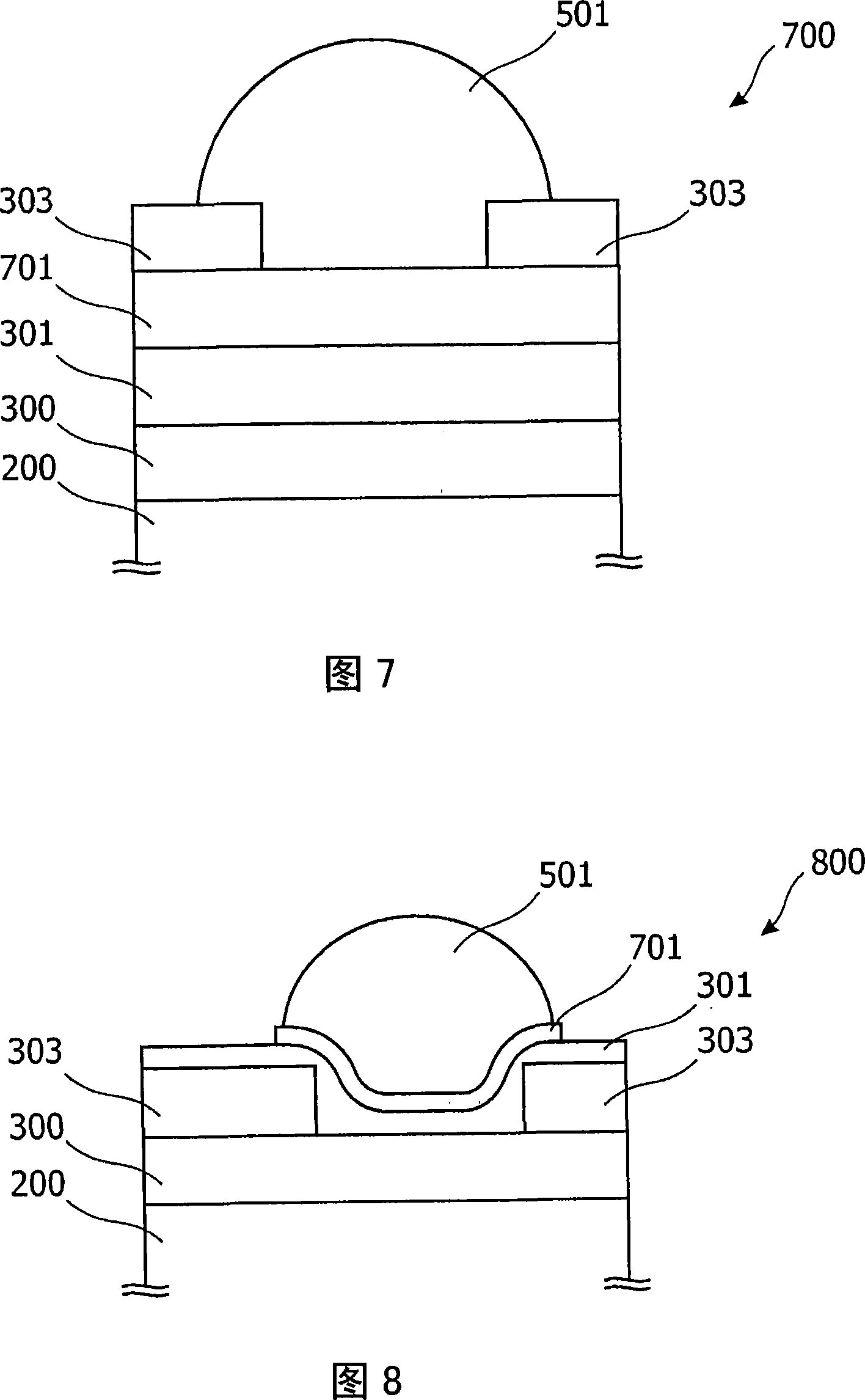
[0059] The illustrations in the figures are schematic. In different figures, similar or identical elements are provided with the same reference signs.
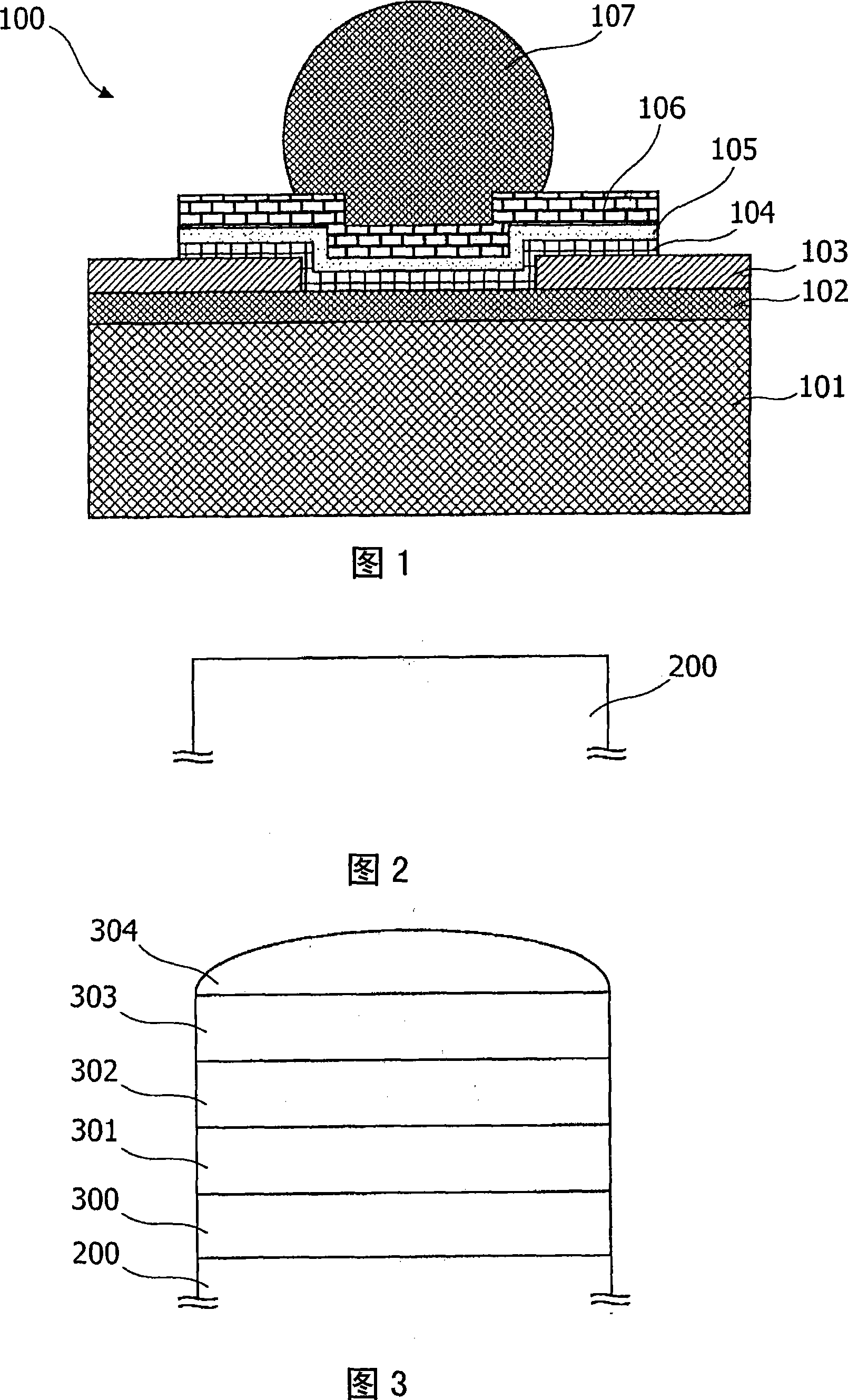
[0060] Hereinafter, referring to FIG. 1 , the layer sequence 100 will be described.
[0061] The layer sequence 100 comprises a semiconductor chip component 101 on which an interconnect metal layer 102 is applied. A passivation layer 103 is deposited and patterned on the interconnect metal layer 102 . Also, an aluminum layer 104 is deposited on the interconnection metal layer 102 and the passivation layer 103 . Further, a nickel / vanadium layer 105 is deposited on the aluminum layer 104 . Also, a copper layer 106 is deposited on the nickel / vanadium layer 105 . Then, lead-containing or lead-free solder balls 107 are applied on the copper layer 106 .
[0062] Referring to FIG. 1 , UBM (Under Bump Metallization) is used as an interconnection layer for preformed solder balls. A metallization stack is created from Al / NiV / Cu (l...
PUM
 Abstract
Description
Claims
Application Information


