Heterojunction bipolar transistor and preparation method thereof

A heterojunction bipolar and transistor technology, applied in semiconductor/solid-state device manufacturing, semiconductor devices, electrical components, etc., can solve problems affecting yield, device failure, metal electrode punch-through, etc.

Inactive Publication Date: 2008-06-25
INST OF SEMICONDUCTORS - CHINESE ACAD OF SCI
View PDF0 Cites 8 Cited by
  • Summary
  • Abstract
  • Description
  • Claims
  • Application Information

AI Technical Summary

Problems solved by technology

In the prior art double-mesa HBT device, because the base region is relatively thin, punch-through is prone to

Method used


Image

  • Heterojunction bipolar transistor and preparation method thereof
  • Heterojunction bipolar transistor and preparation method thereof
  • Heterojunction bipolar transistor and preparation method thereof

Examples


Embodiment Construction

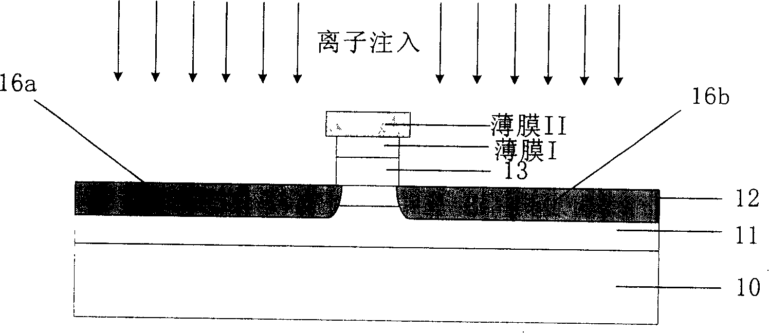
[0041] The heterojunction bipolar transistor and its preparation method of the present invention are characterized in that the outer base region is doped by combining the over-corrosion self-alignment process and ion implantation process, the effect is to reduce the series resistance of the base region and increase The thickness of the ohmic contact area in the base area ensures sufficient alloying and improves the yield.

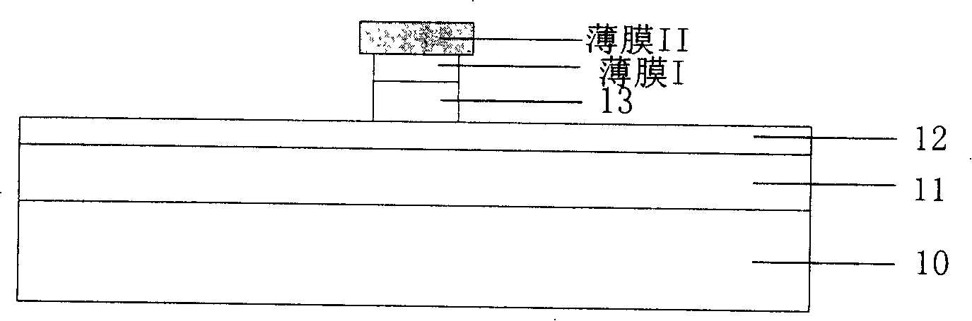
[0042] The heterojunction bipolar transistor of the present invention includes:

[0043] Substrate;

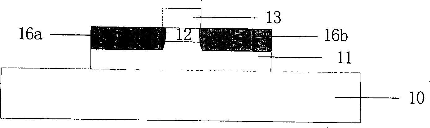
[0044] a collector region of the first doping type on the substrate, the collector region comprising a collector region and a collector contact region;

[0045] a base region of the second doping type on the collector region, wherein the extrinsic base region is thickened by an over-etch self-aligned ion implantation process;

[0046] an emitter region of the first doping type on the base region, the emitter region comprising an emitter region and an emit...


PUM


Abstract

The invention relates to a heterojunction bipolar transistor, which comprises a substrate, a first doping type of collecting electrode area on the substrate, the collecting electrode area comprises a collecting area and a collecting electrode contact area; a second doping type of base electrode area on the collecting electrode area ; a first doping type of emitting electrode area on the base electrode area, an emitting electrode area comprises an emitting area andanemitting electrode cap layer area; the electrode on the emitting electrode cap layer area, the base electrode area and the collecting electrode contact area;, the first doping type is contrary to the second doping type; and the doping type of the ion injected into the outer base area is identical to the second doping type. In the invention the outer base area is adulterated by combining the wet-etching self-aligning process and the ion implantation process, the effect is as following that the base series resistance is reduced, simultaneously the thickness of the base ohmic contact area is increased, the adequacy of alloy is ensured, and the rate of finished products is improved.

Description

technical field [0001] The invention relates to the field of semiconductors, in particular to a heterojunction bipolar transistor structure. [0002] The present invention also relates to a preparation method of the aforementioned heterojunction bipolar transistor. technical background [0003] In recent years, due to the introduction of energy band engineering, heterojunction devices have performance advantages that cannot be replaced by homojunction devices, and have received widespread attention and rapid development. In particular, heterojunction bipolar transistors (HBTs) have the advantages of good threshold uniformity, single-supply operation, superior high-frequency performance, strong current drive performance, and good linearity, and have been widely used in the communication field. [0004] Currently prepared heterojunction transistors have various structures, including mesa structures, planar structures, and the like. There are also various preparation methods,...

Claims


Application Information

Patent Timeline
IPC IPC(8): H01L29/737H01L21/331
Inventor 姚飞薛春来成步文王启明
Owner INST OF SEMICONDUCTORS - CHINESE ACAD OF SCI
Why Eureka
Try Eureka