Method for etching conductive composite layer

A composite layer and photoresist layer technology, which is applied in the manufacture of circuits, electrical components, semiconductors/solid-state devices, etc., can solve the problems of low chip yield, low etching pressure, and small etching rate, etc., and achieve chip yield Improvement, high etching rate, and smooth profile

Inactive Publication Date: 2010-10-13
SEMICON MFG INT (SHANGHAI) CORP
View PDF6 Cites 0 Cited by
  • Summary
  • Abstract
  • Description
  • Claims
  • Application Information

AI Technical Summary

Problems solved by technology

[0008] In prior art etching of the conductive composite layer, due to the low etching pressure of the reaction chamber, which is 6-10 mTorr, the plasma concentration in the reaction chamber is low, so that the selection ratio of the etching gas to etch the conductive composite layer and the silicon oxide layer is small , the selection ratio of etching the conductive composite layer and the photoresist layer is also small, resulting in uneven cross-section of the final semiconductor device, and poor verticality of the sidewall of the trench or contact hole; at the same time, due to the low etching pressure of the reaction chamber, the etching The speed is also correspondingly reduced, resulting in a long time for making semiconductor devices, which in turn makes the chip yield low

Method used


Image

  • Method for etching conductive composite layer
  • Method for etching conductive composite layer
  • Method for etching conductive composite layer

Examples


Embodiment Construction

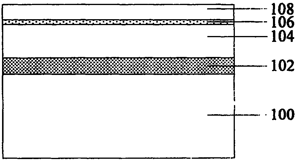
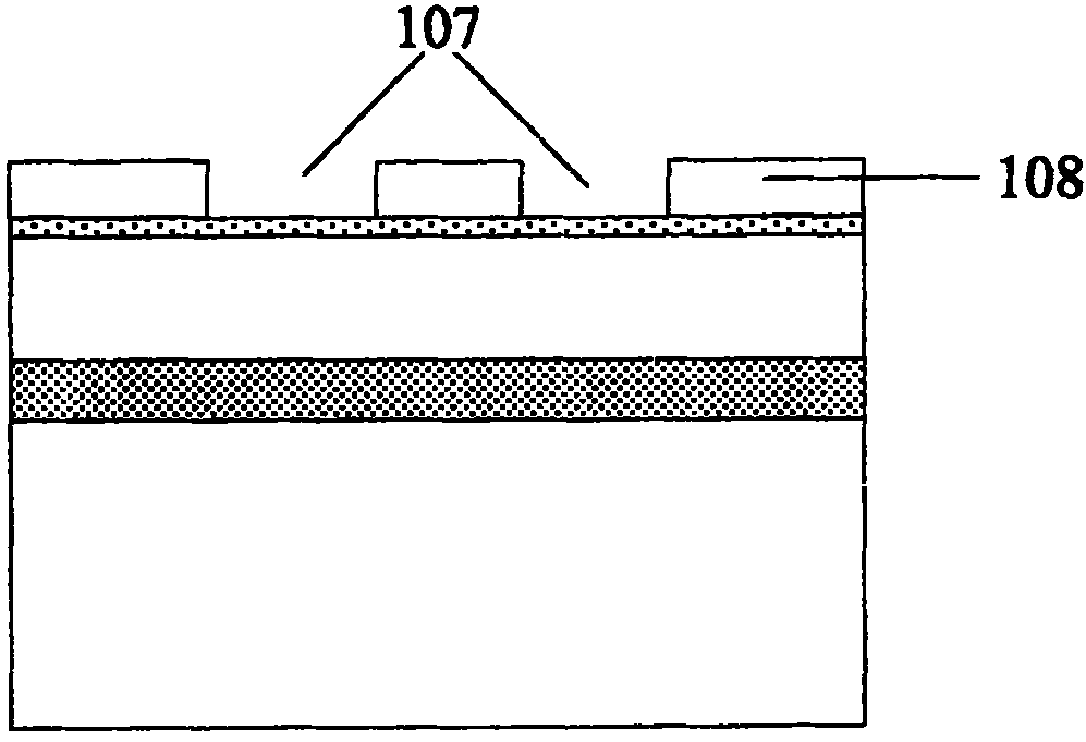
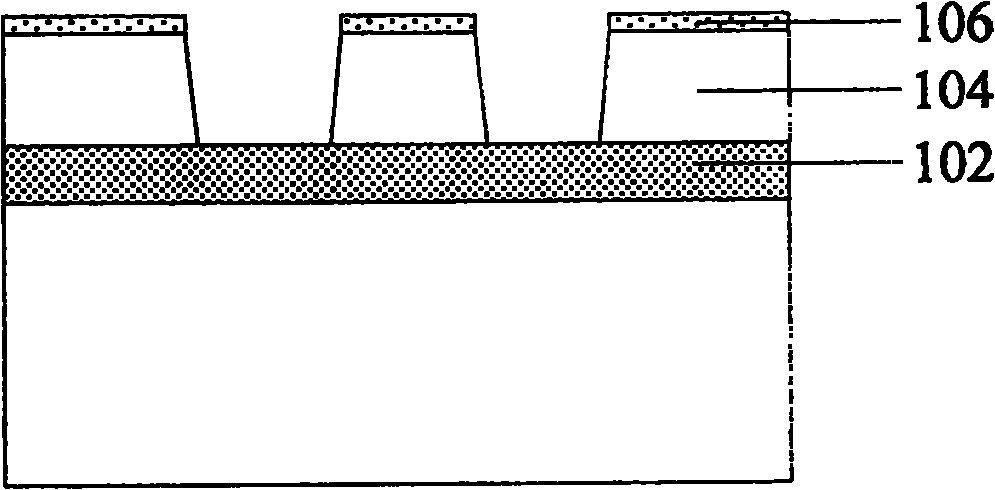
[0022] The invention increases the etching pressure of the reaction chamber from 6 to 10 mTorr to 10 to 30 mTorr, and the plasma concentration in the reaction chamber will also increase accordingly, so that the etching gas can etch the conductive composite layer and the silicon oxide layer The selection ratio of the etching conductive composite layer and the photoresist layer are correspondingly increased, so that the cross section of the finally formed semiconductor device is flat, and the sidewall verticality of the trench or contact hole is good; at the same time, due to the increase of the etching pressure If the etching rate is large, the etching rate will be correspondingly increased, and the time for making semiconductor devices will be shortened, thereby increasing the chip yield. In order to make the above objects, features and advantages of the present invention more comprehensible, specific implementations of the present invention will be described in detail below in...


PUM

PropertyMeasurementUnit
thicknessaaaaaaaaaa
thicknessaaaaaaaaaa
thicknessaaaaaaaaaa

Abstract

A method for etching a conductive composite layer comprises the following steps that: an oxygen ambient silica layer, the conductive composite layer and a nano-pattern photoresist layer are formed on a silicon substrate in order and the silicon substrate with the oxygen ambient silica, the conductive composite layer and the nano-pattern photoresist layer is put in an etching reaction chamber; theetching pressure in the reaction chamber is increased from 6 millitorr - 10 millitorr to 10 millitorr - 30 millitorr and the conductive composite layer is etched till the oxygen ambient silica is exposed with the nano-pattern photoresist layer as mask. After the steps, the semiconductor device formed at last has leveled profile, the verticality of the side wall of the groove or contact hole is good, and the time for making the semiconductor device is shortened so as to further enhance the yield of the chip.

Description

technical field [0001] The invention relates to a manufacturing method of a semiconductor device, in particular to a method for etching a conductive composite layer during the manufacturing of a semiconductor device. Background technique [0002] For the electrodes and interconnection lines of integrated circuits, a conductive composite layer with a thickness of 2 μm is sufficient. However, for silicon-based spiral inductors, in order to improve the quality factor, it is urgent to reduce the series resistance of the metal spiral coil, so a thickness greater than 2 μm is used. The metal layer (hereinafter referred to as thick metal) is more favorable; for example, in special power devices and circuits, thick metal is often used to reduce resistance and improve heat dissipation. Although wet etching can etch thick metal, due to the isotropy of its etching rate, the line accuracy and sidewall morphology cannot be guaranteed. Therefore, it is imperative to develop high-precisio...

Claims


Application Information

Patent Timeline
Patent Type & Authority Patents(China)
IPC IPC(8): H01L21/3213
Inventor 崔红星陈骏傅海林杨渝书
Owner SEMICON MFG INT (SHANGHAI) CORP
Why Eureka
Try Eureka