Method for manufacturing a leadframe, packaging method for semiconductor element and semiconductor package product

A lead frame and semiconductor technology, applied in the fields of semiconductor/solid-state device manufacturing, semiconductor devices, semiconductor/solid-state device components, etc., can solve the problems of long product delivery, high cost, and difficulty in reducing power consumption of radio frequency and analog circuits. Achieve the effect of shortening the signal path, saving lead pins, and improving electronic characteristics

Inactive Publication Date: 2008-07-02
MEDIATEK INC
View PDF0 Cites 2 Cited by
  • Summary
  • Abstract
  • Description
  • Claims
  • Application Information

AI Technical Summary

Problems solved by technology

If such a high-speed semiconductor chip is packaged in a lead frame, the signal loss or AC noise will obviously affect the chip operation performance and become an annoying problem
[0005] The disadvantage of the aforementioned BGA package is its higher cost and longer lead times
In addition, one of the challenges in developing RF SoCs is that it is difficult to reduce the power consumption of RF and analog circuits and reduce the size of passive components and analog transistors

Method used


Image

  • Method for manufacturing a leadframe, packaging method for semiconductor element and semiconductor package product
  • Method for manufacturing a leadframe, packaging method for semiconductor element and semiconductor package product
  • Method for manufacturing a leadframe, packaging method for semiconductor element and semiconductor package product

Examples


Embodiment Construction

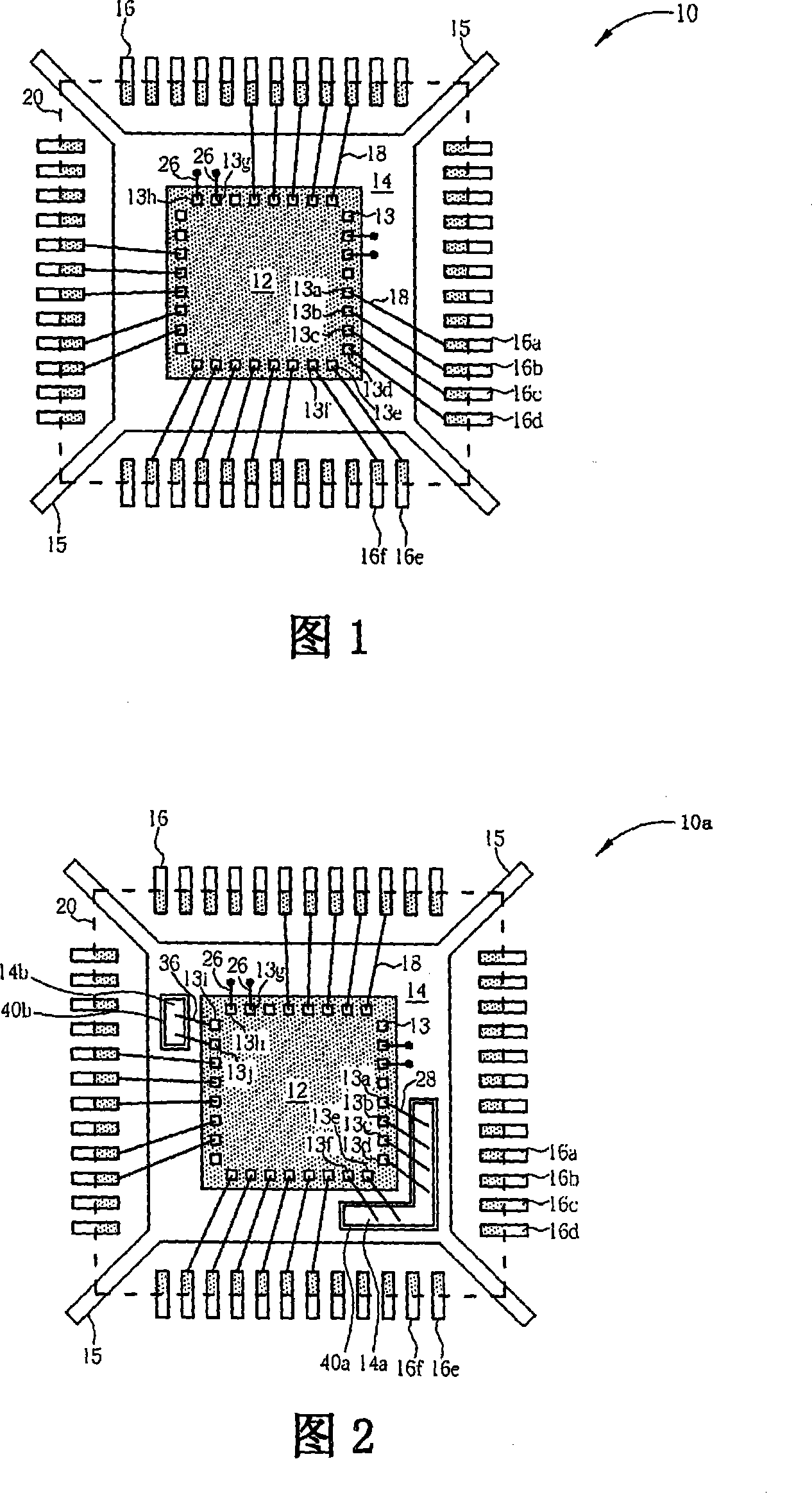
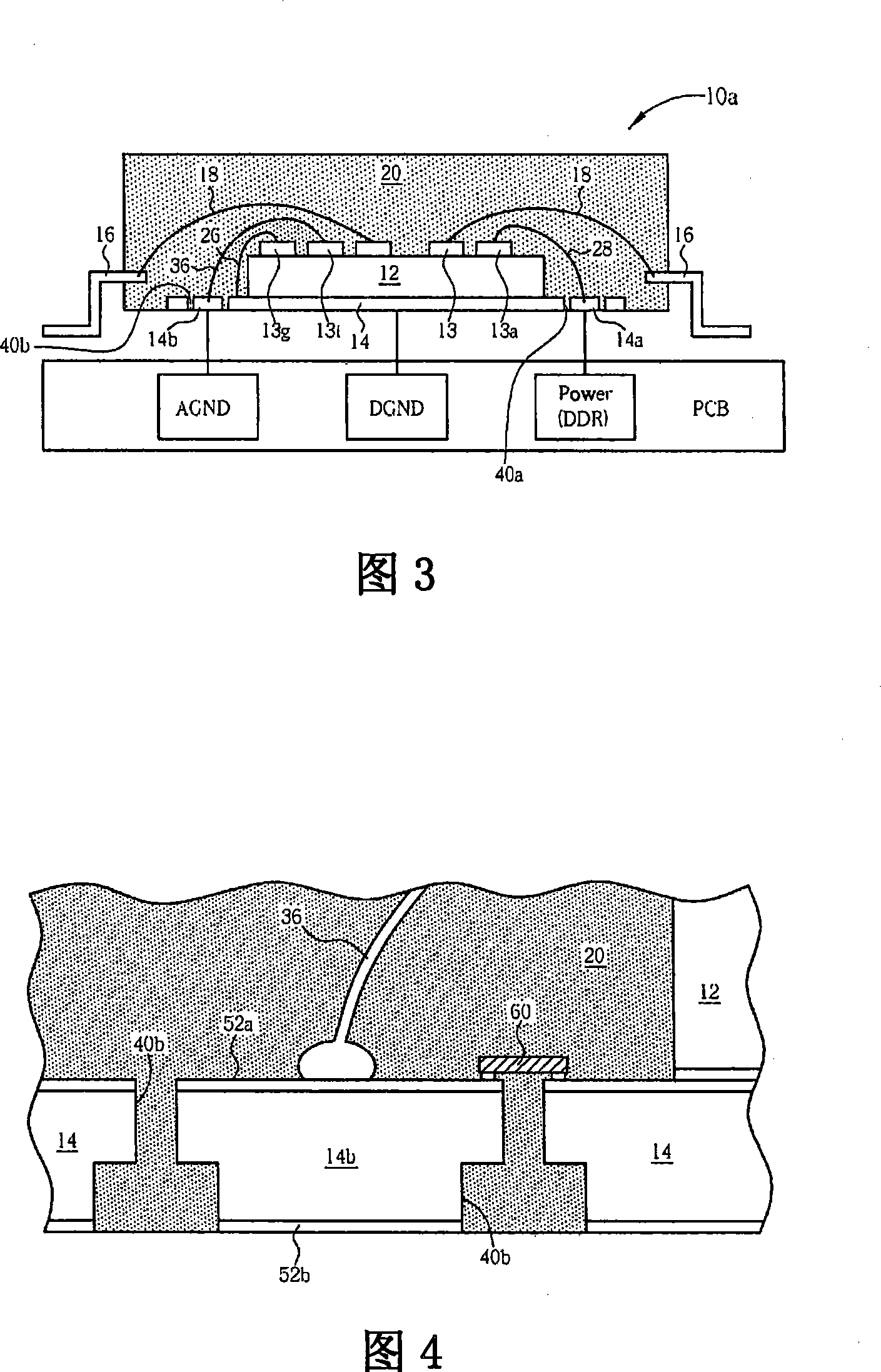
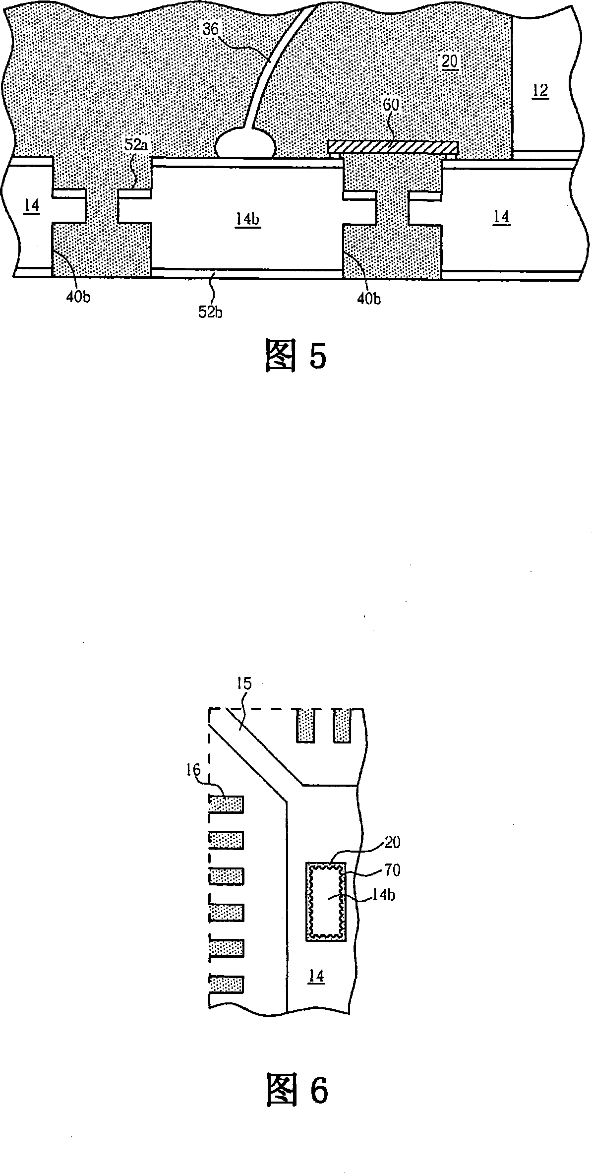
[0032] The leadframe (leadframe) package (packaging) structure described below can be used for, but not limited to, low-profile quad flat pack (LQFP) package, thin quad flat pack (Thin Quad Flat Pack, TQFP) package , Quad Flat Non-leaded (QFN) package, DFN package, multi-zone QFN (multi-zone QFN) package, multi-die package, and flip-chip packaging ).

[0033] Compared with the prior art, by saving or releasing the lead pads (ground pads), power pads (power pads) or other types of signal pads originally used to connect semiconductor chips, the present invention can Pushing the limits of leadframe structure packaging even further. In addition, the present invention can also be used to improve the electronic performance of integrated circuit packaged products by using a separate ground system on the die pad.

[0034] FIG. 1 illustrates a schematic top view of a leadframe package 10 . As shown in FIG. 1 , the lead frame package 10 includes a semiconductor die 12 as an example o...


PUM


Abstract

A leadframe package includes a die pad with four unitary, outwardly extending slender bars; a plurality of leads arranged along periphery of the die pad; a separate pad segment separated from the die pad and isolated from the plurality of leads; a semiconductor die mounted on an upper side of the die pad, wherein the semiconductor die contains first bond pads wire-bonded to respective the plurality of leads and a second bond pad wire-bonded to the separate pad segment; and a molding compound encapsulating the semiconductor die, the upper side of the die pad, the first suspended pad segment and inner portions of the plurality of leads.

Description

technical field [0001] The present invention relates to a lead frame structure for semiconductor devices, in particular to a lead frame packaging component with multiple exposed die pads and a manufacturing method thereof. Background technique [0002] As known to those skilled in the art, in order to avoid the interference and damage of external environmental factors, the semiconductor chip is usually covered with plastic material to form a packaging component. The packaging component also provides the electrical connection between the semiconductor die and the printed circuit board. Such integrated circuit packaging components generally include a metal lead frame, a semiconductor chip disposed on a die mount integrally formed with the metal lead frame, and gold wires electrically connecting the bonding pads on the semiconductor chip with each pin of the lead frame. The semiconductor chip and the lead frame are finally covered by the molding compound. [0003] The current...

Claims


Application Information

Patent Timeline
IPC IPC(8): H01L21/50H01L21/60H01L21/56H01L21/48H01L23/495H01L23/31
CPCH01L2924/01015H01L2224/85476H01L2924/01023H01L2924/19105H01L2924/01046H01L2924/01082H01L2924/0105H01L23/49531H01L2224/85478H01L2224/16H01L2924/30105H01L23/49582H01L2924/01044H01L2924/01029H01L2224/85455H01L2924/01028H01L2224/16245H01L2224/85439H01L2224/48091H01L25/16H01L2224/49171H01L2924/014H01L2924/19015H01L2924/30107H01L2224/85469H01L24/49H01L2924/18301H01L23/49575H01L2224/49173H01L2924/01047H01L2924/01079H01L24/48H01L2224/48247H01L2924/01076H01L2924/14H01L23/49548H01L2924/01033H01L2224/85473H01L2924/19042H01L2924/01006H01L23/66H01L2224/85464H01L2924/01078H01L2224/48257H01L2924/01075H01L2224/85444H01L2224/49175H01L2924/01077H01L21/4832H01L2224/48137H01L2224/05554H01L2924/181H01L2924/00014H01L2224/73265H01L2924/10162H01L2224/49433H01L2924/00H01L2224/45099H01L2924/00012
Inventor 陈南璋林泓均
Owner MEDIATEK INC
Why Eureka
Try Eureka