A kind of wafer-level test probe card and wafer-level test probe card assembly method

A test probe, wafer-level technology, used in measurement devices, electronic circuit testing, measurement of electricity and other directions, can solve the problem of difficult to distribute power supply decoupling, signal noise reduction filter impedance matching, ground potential unequal signal insertion loss probe Card test performance, difficulty in ensuring capacitor placement space, etc., to improve power integrity and signal integrity, improve overall test performance, and reduce dielectric loss

Active Publication Date: 2022-03-08
MAXONE SEMICON CO LTD
View PDF5 Cites 0 Cited by
  • Summary
  • Abstract
  • Description
  • Claims
  • Application Information

AI Technical Summary

Problems solved by technology

With the continuous development of semiconductor technology and the continuous increase of chip operating frequency, problems such as power integrity problems, ground bounce problems, unequal ground potentials, and excessive signal insertion loss have more and more impacts on the test performance of probe cards. Large; as the density of pads on the wafer continues to increase, all types of probes are connected to the substrate, resulting in a small remaining space on the substrate, making it difficult to distribute processing devices and circuits such as power decoupling, signal noise reduction filtering, and impedance matching. , the probes carrying different signals will interfere with each other, affecting the overall test results
[0004] Taking noise filtering as an example, the patent CB105510649A provides a technical means to filter out signal noise by distributing capacitance on the edge of the substrate to solve the problem that the wiring substrate is difficult to ensure enough capacitor placement space
However, this method can only partially solve the problem, and since the capacitance is distributed on the edge of the signal substrate and is relatively far away from the signal pin, there is still room for further improvement in the noise filtering effect

Method used


Image

  • A kind of wafer-level test probe card and wafer-level test probe card assembly method
  • A kind of wafer-level test probe card and wafer-level test probe card assembly method
  • A kind of wafer-level test probe card and wafer-level test probe card assembly method

Examples


specific Embodiment approach 1

[0063] The following are specific implementations of the wafer-level test probe card of the present invention.

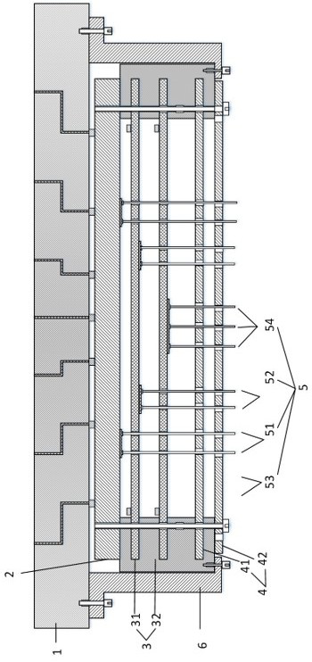
[0064] The wafer-level test probe card under the present embodiment, such as Figure 1-5 As shown, it includes PCB board 1, signal adapter board 2 and probe 5, and also includes intermediary board group 3, guide board group 4 and spacer board group 6;

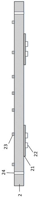
[0065] The surface of the signal transfer board 2 is distributed with a patterned signal transfer board metal interconnection layer 21, a signal transfer board connection structure 22, a signal transfer board signal interface 23 and a signal transfer board pin fixing hole 24; The signal adapter board connection structure 22 is located on the metal interconnection layer 21 of the signal adapter board, and is used to realize the connection between the signal adapter board metal interconnection layer 21 and the probe 5;

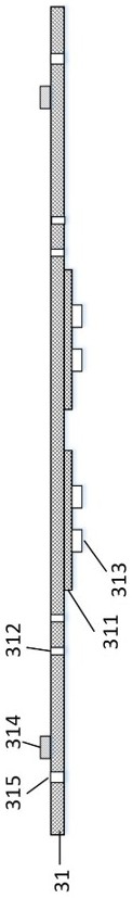
[0066] The interposer group 3 includes a top interposer 31 and a bottom interposer 32, the surface...

specific Embodiment approach 2

[0072] The following are specific implementations of the wafer-level test probe card of the present invention.

[0073] The wafer-level test probe card under this embodiment is further defined on the basis of Embodiment 1: the surface and interior of the signal adapter board 2, the top interposer 31 and the bottom interposer 32 are based on the probes accommodated. 5 types, distributed with power supply decoupling capacitors, signal filtering and noise reduction circuits and / or impedance matching circuits.

specific Embodiment approach 3

[0074] The following are specific implementations of the wafer-level test probe card of the present invention.

[0075] The wafer-level test probe card under this embodiment is further defined on the basis of the first embodiment: the signal interface 23 of the signal adapter board, the signal interface 314 of the top interposer and the signal interface 324 of the bottom interposer are connected to Signal types include power signals, ground signals, low frequency test signals, or high frequency test signals.


PUM


Abstract

A wafer-level test probe card and a wafer-level test probe card assembly method of the present invention belong to the technical field of probe cards and wafer testing; the wafer-level test probe card includes a PCB board, a signal adapter board and a probe card. needle, also includes interposer group, guide plate group and spacer group; described interposer group includes top interposer, bottom interposer and low power consumption interposer, and described probe includes power supply probe, ground probe, There are four kinds of low-frequency signal probes and high-frequency signal probes, which are respectively connected to the signal adapter board and the interposer board group; the assembly method of the wafer-level test probe card uses this to perform the following steps: align the pinholes, place the pins, probe Needle limit and PCB connection; the present invention provides sufficient accommodation space for signal decoupling, anti-interference, noise reduction and other processing circuits through grouping of probes, which can isolate or reduce the coupling and interference between different signal probes, and improve the reliability of the system. The overall test performance, especially, can improve the high frequency test capability of the system.

Description

technical field [0001] The invention discloses a wafer-level test probe card and a method for assembling the wafer-level test probe card, belonging to the technical field of probe cards and wafer testing. Background technique [0002] Wafer testing is to detect the electrical characteristics of each die on the wafer, eliminate unqualified die early or optimize product design, and avoid cost waste caused by packaging of defective products. The probe card is a test device used for wafer inspection. By transmitting the test signal of the test machine to the object under test, and sending the response signal of the object under test back to the test machine through itself, the performance of the chip can be optimized. Testing, in conjunction with other testing and analysis instruments, can realize a complete test of the pros and cons of chips and performance, realize the screening of defective products, and reduce unnecessary packaging costs. [0003] During the test, the test ...

Claims


Application Information

Patent Timeline
Patent Type & Authority Patents(China)
IPC IPC(8): G01R31/28G01R1/073G01R3/00
CPCG01R31/2886G01R31/2831G01R1/07307G01R3/00
Inventor 赵梁玉于海超
Owner MAXONE SEMICON CO LTD
Why Eureka
Try Eureka