Semiconductor device with gate structure and method for fabricating the semiconductor device
A gate structure, semiconductor technology, applied in semiconductor/solid-state device manufacturing, semiconductor devices, electrical components, etc., can solve problems such as device characteristic degradation
- Summary
- Abstract
- Description
- Claims
- Application Information
AI Technical Summary
Problems solved by technology
Method used
Image

Examples
Embodiment Construction
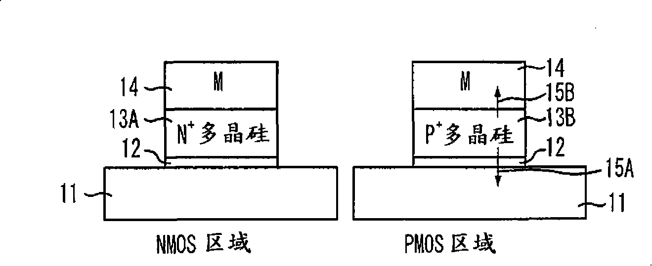
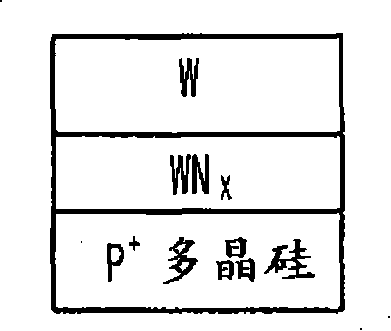
[0028] Figure 3A ~ 3C The gate structures of PMOS devices each including a specific intermediate structure are illustrated. Figure 3A illustrated with a tungsten nitride (WN x ) single-layer gate structure. Figure 3B Illustrations that have included WSi x and WN x double-layer gate structure. Figure 3C Illustrated with titanium (Ti), titanium nitride (TiN x ) and WN x The three-layer gate structure. Here, x indicating the corresponding atomic ratio is a positive number. exist Figure 3A ~ 3C , each gate structure consists of a P + An electrode formed of polysilicon doped with type impurities and a metal electrode formed of W.
[0029] The gate structures of PMOS devices with different intermediate structures exhibit different characteristics. For intermediate structures containing a single layer, such as Figure 3A As shown, a Si-N dielectric layer may be formed on the interface of the polysilicon electrode. Therefore, the contact resistance of the gate struct...
PUM
 Abstract
Description
Claims
Application Information