Luminous diode device structure and its manufacture method

A technology for light-emitting diodes and device structures, applied in semiconductor devices, electrical components, circuits, etc., can solve problems such as affecting the anti-static performance of devices and reducing crystal quality

Active Publication Date: 2008-07-02
EPILIGHT TECH
View PDF0 Cites 22 Cited by
  • Summary
  • Abstract
  • Description
  • Claims
  • Application Information

AI Technical Summary

Problems solved by technology

The existing relatively common roughening process is to grow the GaN layer at low temperature, but the low temperature proc

Method used


Image

  • Luminous diode device structure and its manufacture method

Examples


Embodiment Construction

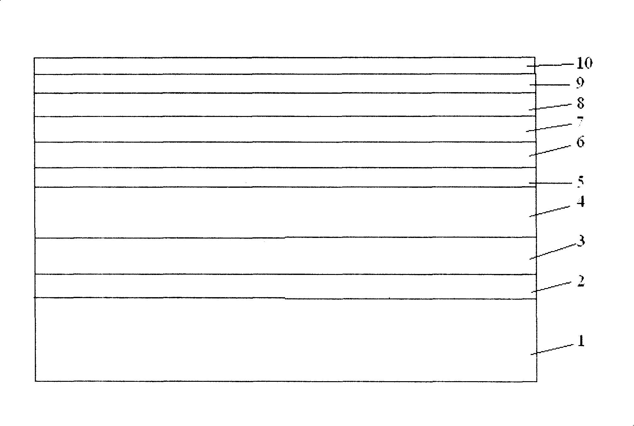
[0021] The structure of the light-emitting diode device of the present invention can be referred to as shown in the accompanying drawings, including the following layers from bottom to top: sapphire substrate 1, buffer nucleation layer 2, undoped GaN layer 3, N-type GaN layer, multiple quantum wells Layer 7, Al and Mg-doped GaN layer 8 and Mg-doped GaN layer, the N-type GaN layer is divided into a first Si-doped GaN layer 4 located below and a second Si-doped GaN layer 6 located above, A Si-doped AlGaN layer 5 is also included between the first Si-doped GaN layer 4 and the second Si-doped GaN layer 6 .

[0022] The total thickness of the first Si-doped GaN layer 4 , the Si-doped AlGaN layer 5 and the second Si-doped GaN layer 6 is 3 μm˜5 μm.

[0023] The Mg-doped GaN layer includes a Mg-doped high-temperature GaN layer 9 located below and a Mg-doped low-temperature GaN layer 10 located above.

[0024] The Mg-doped low-temperature GaN layer 10 is a roughened layer.

[0025] T...


PUM

PropertyMeasurementUnit
Thicknessaaaaaaaaaa
Film thicknessaaaaaaaaaa

Abstract

The invention discloses a structure of a light-emitting diode device, which includes the following layers from the upper part to the lower part in sequence: a sapphire substrate, a buffer nucleation layer, an undoped GaN layer, an N-type GaN layer, a multiple quantum well layer, a GaN layer doped with Al and Mg as well as a GaN layer doped with the Mg. The N-type GaN layer is respectively arranged on a lower first GaN layer doped with Si and an upper second GaN layer doped with the Si. An AlGaN layer doped with the Si is contained between the first GaN layer doped with the Si and the second GaN layer doped with the Si. The invention also discloses a method for manufacturing the light-emitting diode device. When the N-type layer is manufactured, the following steps are included: at first, the first GaN layer doped with the Si grows; then, the AlGaN layer doped with the Si grows; at last, the second GaN layer doped with the Si grows. The light-emitting diode device is manufactured by the method provided by the invention and the method has simple steps and easy realization. Furthermore, the manufactured light-emitting diode device has good static-proof capacity and a crystal structure, thus greatly facilitating the performance of the light-emitting diode.

Description

technical field [0001] The invention relates to a semiconductor device structure, in particular to a light emitting diode device structure. The invention also relates to a manufacturing method of the light emitting diode device structure. Background technique [0002] High-brightness light-emitting diodes are increasingly used in display, decorative and landscape lighting applications. However, the harsh conditions of outdoor use put forward higher and higher requirements on the performance of light-emitting diode devices, especially the antistatic ability. Many decorative circuits are series circuits. If one LED is broken, it will cause the LEDs of the entire line to go out. Among light-emitting diodes of various colors, the antistatic ability of blue-green light-emitting diodes made of GaN (gallium nitride) has always been relatively weak. In recent years, Taiwan, Japan, and some domestic companies have invested huge research resources in this area, trying to improve th...

Claims


Application Information

Patent Timeline
IPC IPC(8): H01L33/00
Inventor 付小朝黄宝亿季辉丁晓民朱广敏
Owner EPILIGHT TECH
Why Eureka
Try Eureka