A double-light source laser annealing device and method

A technology of laser annealing and dual light sources, which is applied in the fields of electrical components, semiconductor/solid-state device manufacturing, circuits, etc., can solve the problems that are difficult to meet the requirements of the 65nm node, and achieve the effect of reducing laser energy density and reducing thermal stress

Inactive Publication Date: 2008-07-09
TSINGHUA UNIV
View PDF0 Cites 11 Cited by
  • Summary
  • Abstract
  • Description
  • Claims
  • Application Information

AI Technical Summary

Problems solved by technology

Due to the limitations of thermal diffusion and solid solubility, traditional light rapid thermal annealing (RTA), even with spike annealing technology, is difficult to meet the requirements of the 65nm node

Method used


Image

  • A double-light source laser annealing device and method

Examples


Embodiment Construction

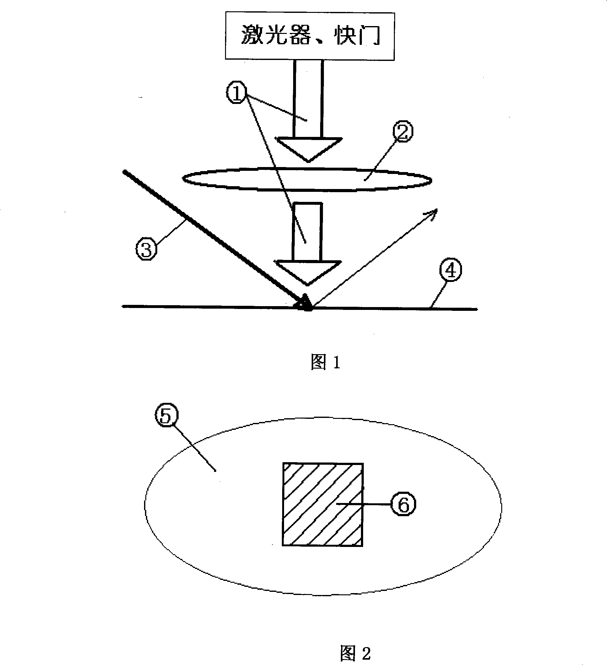
[0031] The invention provides a dual-light source laser annealing device and annealing method. The main structure of the laser annealing device with dual light sources is shown in Figure 1. In Fig. 1, the annealing laser source 1 is incident on the substrate wafer 4 above the wafer stage through the optical lens system 2 to anneal the substrate wafer; the substrate wafer 4 is mounted on the wafer stage Above, along with the film table in the vertical and horizontal directions, step by field, each time the position of the exposure field is moved; one exposure field is equal to the area of ​​one or several chips, and the part of the edge of the exposure field with uneven light intensity Fall in the dicing groove on the edge of the chip; with the stepping of the wafer stage, the entire substrate wafer can be exposed field by field for laser annealing; another auxiliary heating light source of the device shown in Figure 1, auxiliary The heating beam 3 is incident obliquely to the surf...


PUM


Abstract

The invention discloses a dual-light source laser annealing device and a method, which pertains to the semiconductor manufacturing equipment and technical scope. The dual-light source laser annealing device comprises a laser light source for annealing, light sources which have the wavelength of sub-micron to micron scale and are used for auxiliary heating, an optical lens system and a wafer carrier. The processing method is that the oblique incidence of the auxiliary heating light beams reaches the surface of a substrate wafer, and the pre-heating is carried out at the substrate surface before the formal laser annealing, so as to improve the adverse effects of the thermal stress on the annealing and the wafer surface appearance. On the other hand, as the processing of pre-heating, a great number of phonons are introduced to a superficial surface layer of the substrate wafer, the existence of the phonons can be conductive to the relaxation of carrier energy and obtain better annealing effect, so the temperature raise of a crystal lattice and the annealing process of the wafer can be completed in a shorter time, and the more shallow ultra-shallow junction can also be obtained. Due to the pre-heating of the crystal lattice, the laser energy density which is needed by the laser annealing is also reduced.

Description

Technical field [0001] The invention belongs to the scope of semiconductor manufacturing equipment and technology, and particularly relates to a laser annealing device and method with dual light sources. Background technique [0002] With the continuous shrinking of device size, how to form an advanced ultra-shallow junction (Ultra-Shallow Junction) of the source and drain regions of transistors at 45nm, 32nm and other technology nodes, and even smaller sizes, has become a crucial technical issue. challenge. In order to meet the requirements of ultra-shallow PN junctions for 12" wafers of 45nm and below generations of devices, the traditional rapid thermal annealing (RTA) using strip or spherical lamps as the light source must be changed. For example, it has been carried out. Certainly researched (Spike Annealing) process technology. And a large number of studies have shown that in nano-level CMOS devices, ultra-shallow and low-resistivity junctions play an increasingly important...

Claims


Application Information

Patent Timeline
Patent Type & Authority Applications(China)
IPC IPC(8): H01L21/00H01L21/324
Inventor 严利人周卫刘志弘仲涛
Owner TSINGHUA UNIV
Why Eureka
Try Eureka