Photo-etching machine silicon slice bench double-bench switching system adopting cross slide rail

A cross guide and exchange system technology, which is used in microlithography exposure equipment, semiconductor/solid-state device manufacturing, photolithography process exposure devices, etc., can solve the problems of high system synchronization control requirements and complex structure, and achieve system structure simplification , the effect of reducing requirements

Active Publication Date: 2008-07-16
TSINGHUA UNIV +1
View PDF5 Cites 13 Cited by
  • Summary
  • Abstract
  • Description
  • Claims
  • Application Information

AI Technical Summary

Problems solved by technology

[0009] In view of the shortcomings and defects of the complex structure of the above-mentioned invention application and high requirements for system sync

Method used


Image

  • Photo-etching machine silicon slice bench double-bench switching system adopting cross slide rail
  • Photo-etching machine silicon slice bench double-bench switching system adopting cross slide rail
  • Photo-etching machine silicon slice bench double-bench switching system adopting cross slide rail

Examples


Embodiment Construction

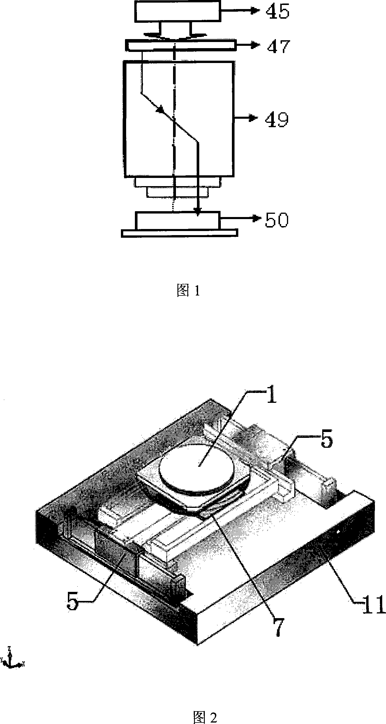
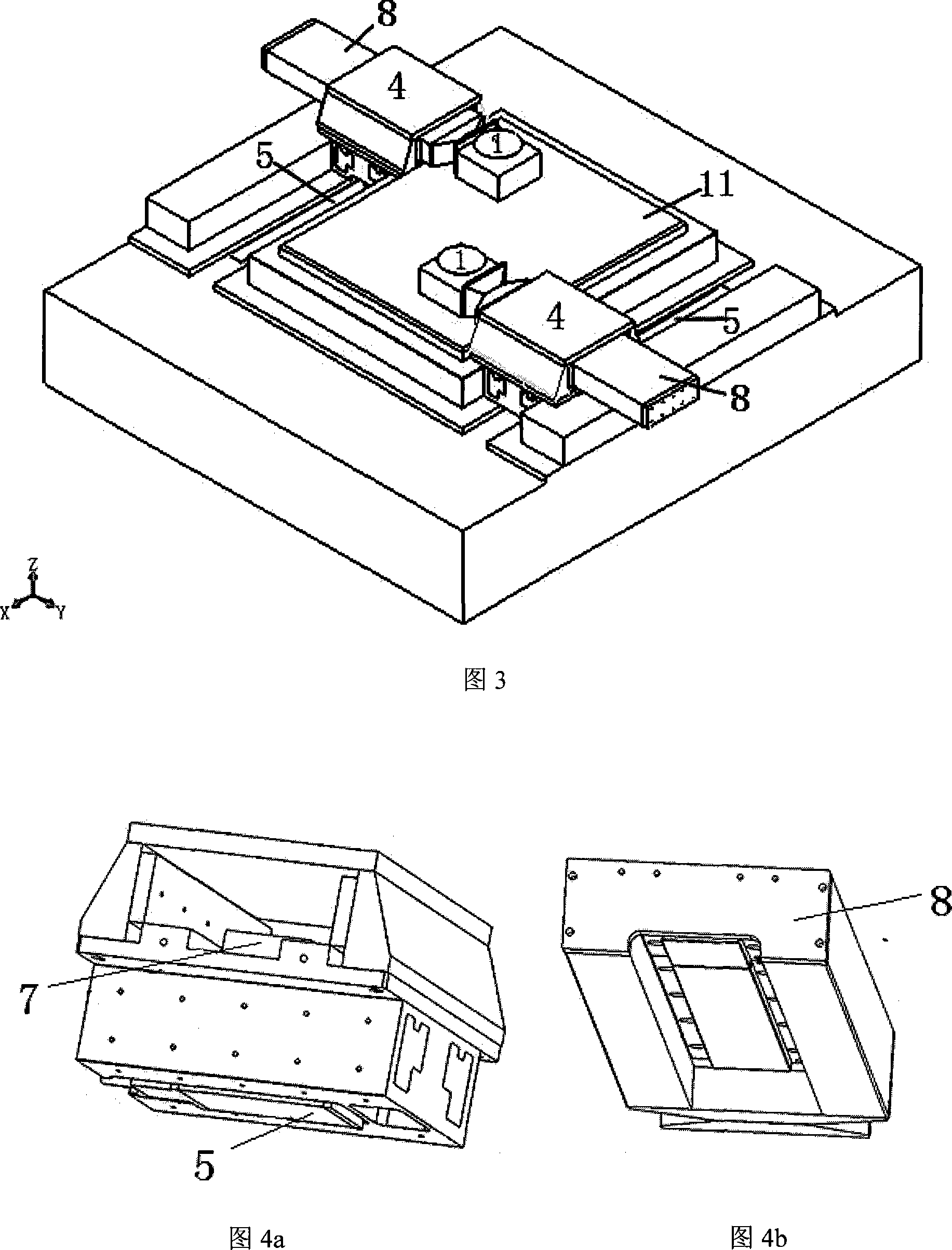
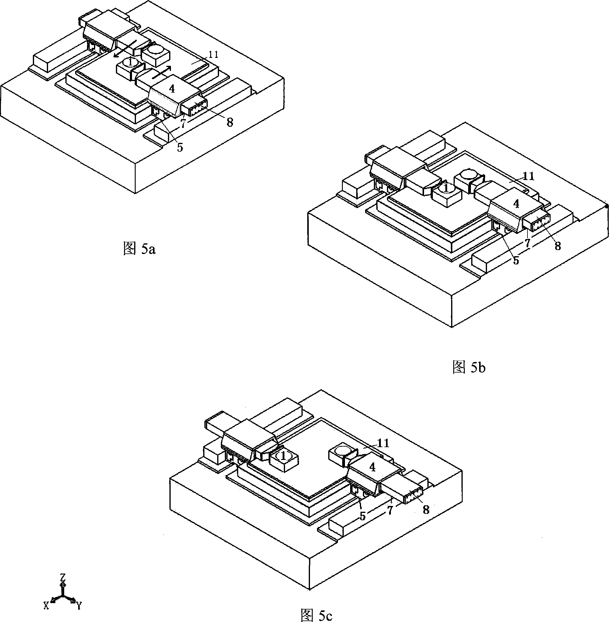
[0021] The silicon wafer stage of a traditional step-and-scan projection lithography machine is shown in Figure 2. There is only one wafer motion positioning system in the lithography machine, that is, only one wafer stage. Preparatory work such as leveling, focusing, and alignment are all done on the same wafer stage. These tasks take a long time, especially alignment, due to the requirement for extremely accurate low-speed scanning (typical alignment The scanning speed is 1 mm / s), so the time required is very long. In order to improve the exposure efficiency of the lithography machine, a simple structure of the lithography machine silicon wafer table rotation exposure system described in the present invention transfers the exposure preparation work such as leveling, focusing and alignment to the silicon wafer in the pretreatment station. On the stage, and work independently with the silicon wafer stage of the exposure station at the same time, thereby greatly shortening the ...


PUM


Abstract

A lithography machine silicon wafer stage double-stage switching system adopting a cross guide rail is mainly used in a semiconductor lithography machine. The invention comprises a silicon wafer stage operating at a pretreatment work station, a silicon wafer stage operating at an exposing work station and two cross guide rail drive units, wherein each cross guide rail drive unit comprises an X-direction linear motor, a Y-direction linear motor and push rods used to push the silicon wafer stages to move; the cross guide rail drive units are caught up with the silicon wafer stages through a vacuum bearing to drive the silicon wafer stages to move within a large scope in X direction and Y direction. The invention adopts two double degree of freedom drive units, thereby greatly simplifying system structure and effectively reducing the requirements of synchronous control.

Description

technical field [0001] The invention relates to a double-stage exchange system for silicon wafer stages of a lithography machine, which is mainly applied to a semiconductor lithography machine and belongs to the technical field of semiconductor manufacturing equipment. Background technique [0002] In the production process of integrated circuit chips, the exposure transfer (photolithography) of the design pattern of the chip on the photoresist on the surface of the silicon wafer is one of the most important processes. The equipment used in this process is called a lithography machine (exposure). machine). The resolution and exposure efficiency of the lithography machine greatly affect the feature line width (resolution) and productivity of integrated circuit chips. As the key system of the lithography machine, the motion accuracy and work efficiency of the silicon wafer ultra-precision motion positioning system (hereinafter referred to as the wafer stage) determine the res...

Claims


Application Information

Patent Timeline
IPC IPC(8): G03F7/20H01L21/68
Inventor 朱煜张鸣汪劲松徐登峰尹文生胡金春杨开明李广闵伟段广洪
Owner TSINGHUA UNIV
Why Eureka
Try Eureka