Peak-hold circuit and signal strength indicator using the peak-hold circuit

A peak hold circuit and signal strength detection technology, which is applied in the direction of improving the amplifier to reduce temperature/power voltage changes, electrical components, and amplification control. It can solve the problem of a large number of circuit components and achieve simple circuit structure and high precision. The effect of simple output and circuit structure

Inactive Publication Date: 2013-05-08
LAPIS SEMICON CO LTD
View PDF1 Cites 0 Cited by
  • Summary
  • Abstract
  • Description
  • Claims
  • Application Information

AI Technical Summary

Problems solved by technology

[0008] However, the gain compensating means and the adjusting means of saturation-limited amplitude, that is, the amplitude control bias generators 131 to 134 have a problem that a large number of circuit components are required as in the specific circuit example described in Patent Document 1.

Method used


Image

  • Peak-hold circuit and signal strength indicator using the peak-hold circuit
  • Peak-hold circuit and signal strength indicator using the peak-hold circuit
  • Peak-hold circuit and signal strength indicator using the peak-hold circuit

Examples


Embodiment 1

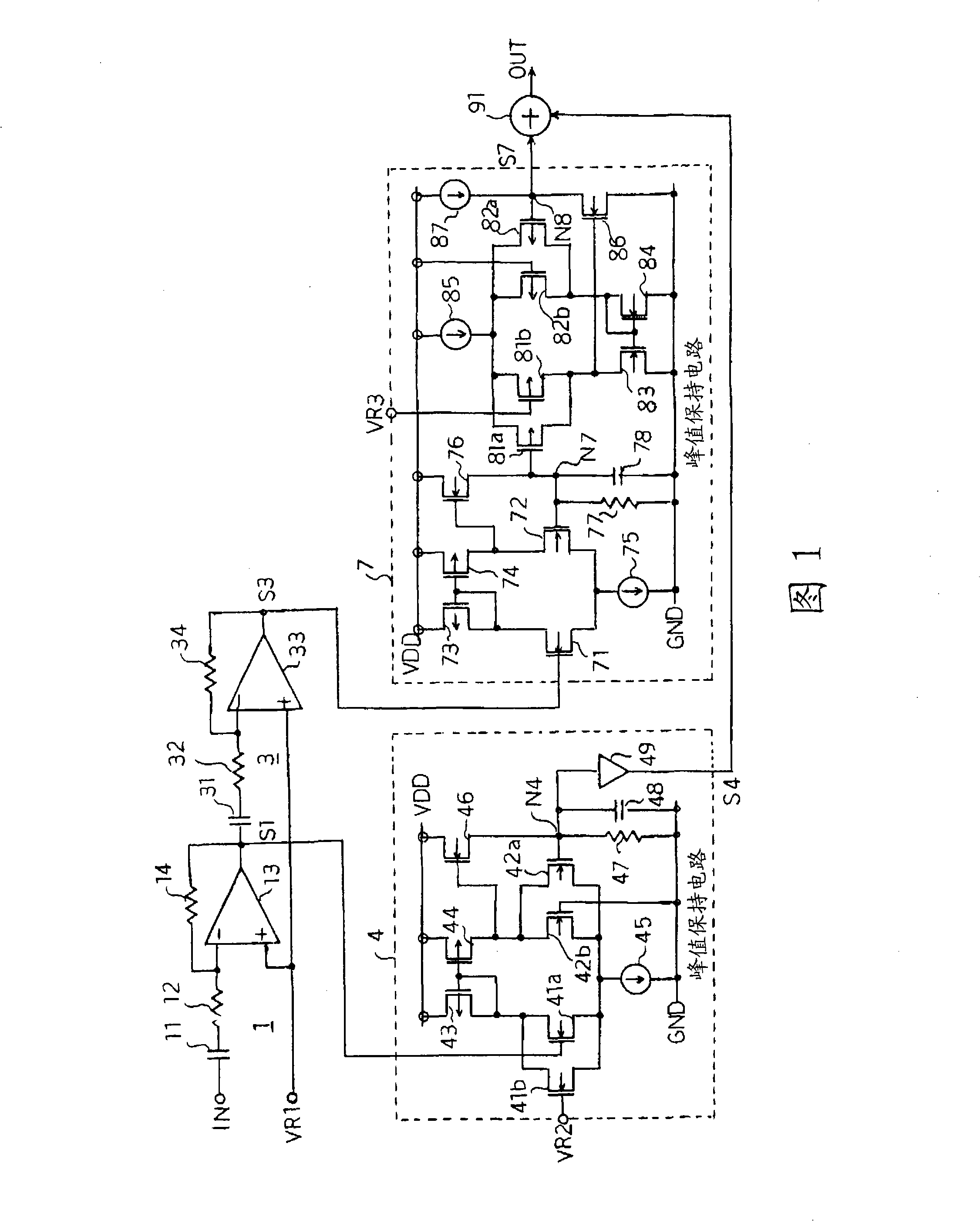
[0025] figure 1 is a configuration diagram showing a signal strength detection circuit according to Embodiment 1 of the present invention.

[0026] This signal strength detection circuit has: 2 stages of cascade-connected amplifying circuits 1, 3; peak holding circuits 4, 7 that hold the peak values ​​of the output signals of the respective amplifying circuits 1, 3; and the outputs of these peak holding circuits 4, 7 Adder 91 where the signals are added.

[0027] The amplifier circuit 1 has an input terminal supplied with an input signal IN, and the input terminal is connected to a negative input terminal of an inverting amplifier 13 via a capacitor 11 and a resistor 12 connected in series. The reference voltage VR1 is supplied to the positive input terminal of the inverting amplifier 13 , and the signal S1 output from the output terminal of the inverting amplifier 13 is fed back to the negative input terminal via the resistor 14 . The amplifying circuit 3 amplifies the sig...

Embodiment 2

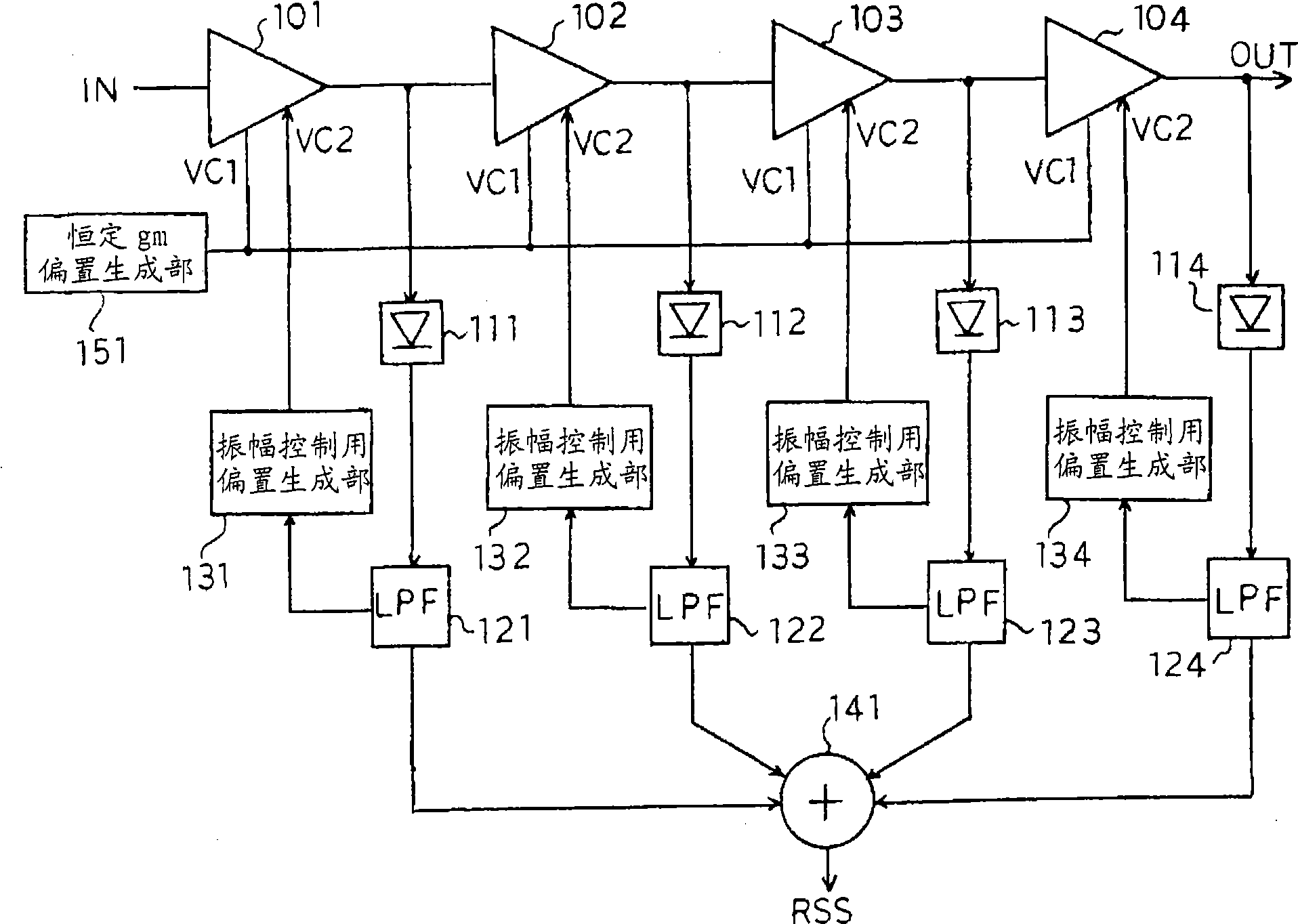
[0071] Figure 7 is a structural diagram showing the signal strength detection circuit of Embodiment 2 of the present invention, and figure 1 Elements common to the elements in are attached with a common symbol.

[0072] The signal strength detection circuit in the figure 1 The intermediate-stage amplifier circuit 2 is inserted between the amplifier circuits 1 and 3 connected in cascade to form a three-stage structure, and a peak hold circuit 5 for holding the peak value of the output signal of the inserted amplifier circuit 2 is provided. Also, an adder 92 for adding the output signals of the peak hold circuits 4, 5, and 7 is provided instead of figure 1 The adder 91 in.

[0073] The amplifier circuit 2 has the same configuration as the amplifier circuits 1 and 3, amplifies the signal S1 supplied from the amplifier circuit 1, and outputs it as a signal S2. Signal S2 is supplied to amplification circuit 3 and is also supplied to peak hold circuit 5 .

[0074] On the ot...


PUM


Abstract

A peak-hold circuit includes a differential amplifier having first and second transistors as a differential pair, the first transistor receiving an input signal at its gate, a third transistor connected between a first power supply and an output node connecting a gate of the second transistor, connectivity of the third transistor being controlled by the output of the differential amplifier, a capacitor for holding a peak voltage, connected between the output node and a second power supply, a resistor for discharging, which is connected in parallel to the capacitor, and a fourth transistor connected to the first transistor in parallel, the fourth transistor receiving at its gate an a reference voltage for limiting a voltage.

Description

technical field [0001] The present invention relates to a peak hold circuit for holding the peak value of an input signal and a signal strength detection circuit using the peak hold circuit. Background technique [0002] figure 2 It is a configuration diagram of a conventional signal strength detection circuit described in Patent Document 1 below. [0003] This signal strength detection circuit is used to detect the strength of a transmission signal and a reception signal in a wireless communication device, etc., and outputs a signal strength RSS based on each output signal of four cascade-connected saturating amplifiers 101 to 104 . [0004] Each of the saturated amplifiers 101 to 104 has two gain control terminals VC1 and VC2. The bias signal generated by the constant gm bias generating unit 151 is supplied to the gain control terminal VC1 so that the saturation amplifiers 101 to 104 of each stage amplify at a constant gain regardless of temperature. On the other hand, ...

Claims


Application Information

Patent Timeline
Patent Type & Authority Patents(China)
IPC IPC(8): H03G3/30H03F1/30H04B1/16
CPCH03F3/45
Inventor 平田学太矢隆士田嶋一行
Owner LAPIS SEMICON CO LTD
Why Eureka
Try Eureka