Semiconductor device and method for fabricating the same

A manufacturing method and semiconductor technology, applied in semiconductor/solid-state device manufacturing, semiconductor devices, transistors, etc., to achieve the effect of eliminating underlying dependencies and improving driving force

Inactive Publication Date: 2008-08-06
PANASONIC CORP
View PDF0 Cites 3 Cited by
  • Summary
  • Abstract
  • Description
  • Claims
  • Application Information

AI Technical Summary

Problems solved by technology

Thus, there arises a problem that the effect of improving the driving force of the MIS transistor obtained by increasing the film thickness of the silicon nitride film as the contact coating film is suppressed.

Method used


Image

  • Semiconductor device and method for fabricating the same
  • Semiconductor device and method for fabricating the same
  • Semiconductor device and method for fabricating the same

Examples


no. 1 example

[0067] Next, the structure of the semiconductor device according to the first embodiment of the present invention will be described with reference to the drawings.

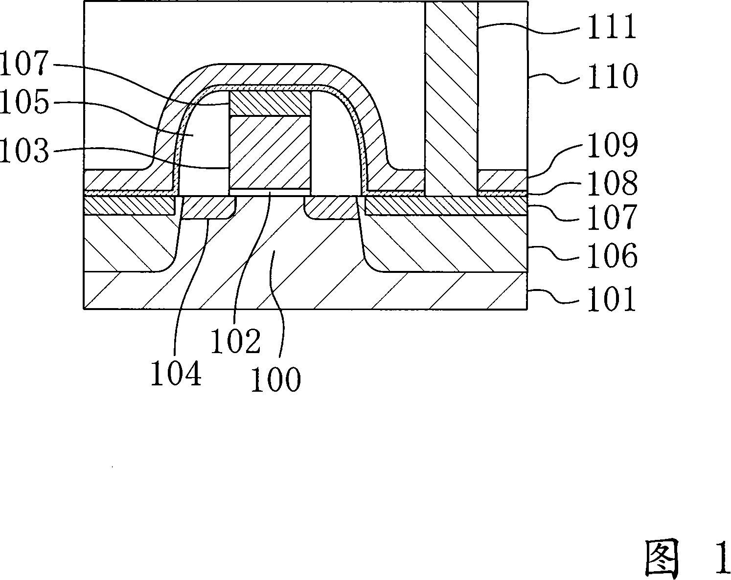
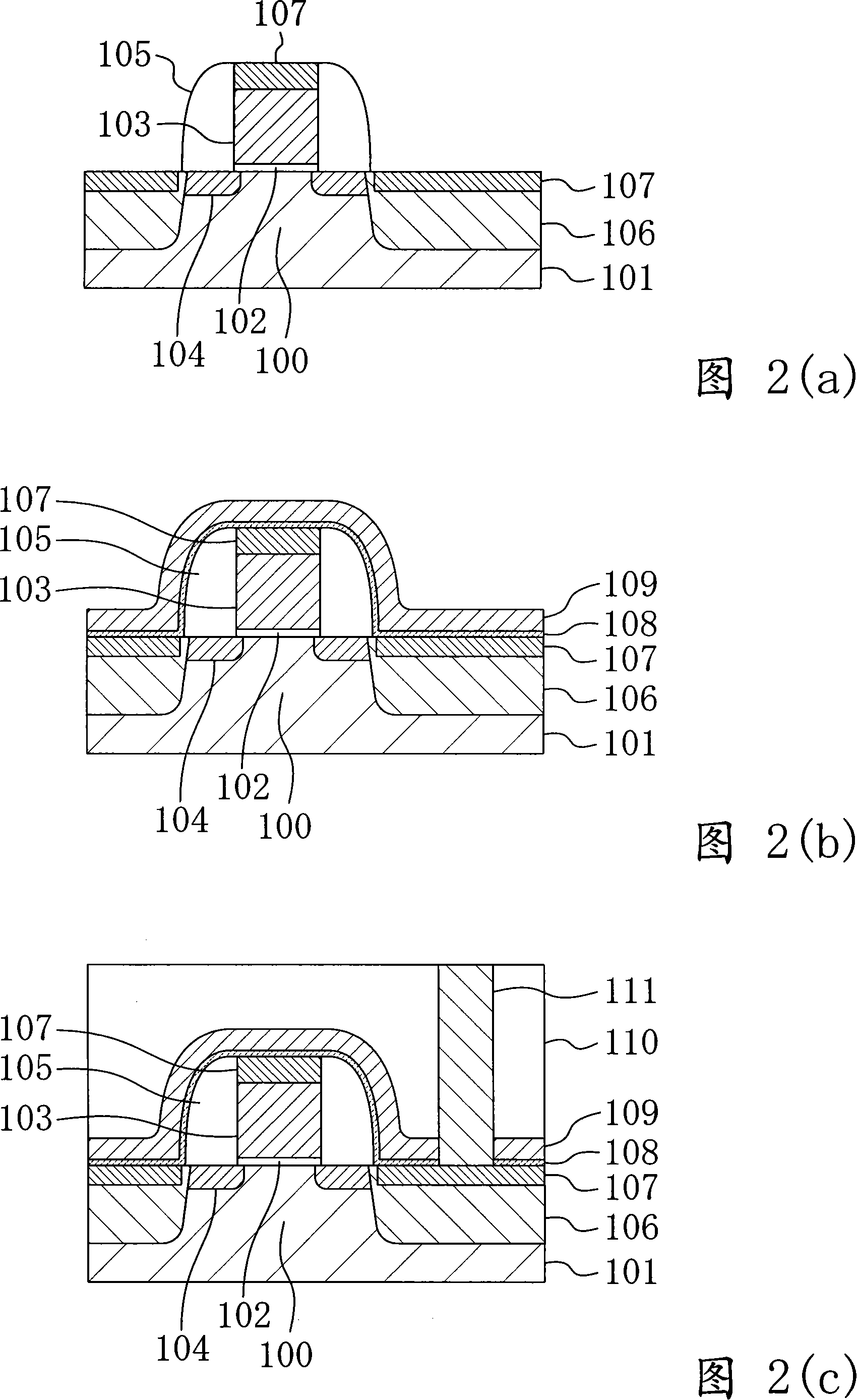
[0068] FIG. 1 is a schematic cross-sectional view showing the structure of a semiconductor device according to a first embodiment of the present invention.

[0069] As shown in FIG. 1 , in a semiconductor substrate 101 made of, for example, silicon, an active region 100 surrounded by an element isolation region (not shown) and having a p well (not shown) is formed, and on the active region 100 A gate electrode 103 having a silicide region 107 made of, for example, NiSi with a film thickness of about 20 nm is formed on an upper layer through a gate insulating film 102 made of, for example, a SiON-based film with a film thickness of about 2 nm. The film thickness of the electrode 103 is about 110 nm. Also, the gate length of the gate electrode 103 is about 50 nm. In the regions on both sides of the gate electrode ...

no. 2 example

[0091] Next, the structure of a semiconductor device according to a second embodiment of the present invention will be described with reference to the drawings.

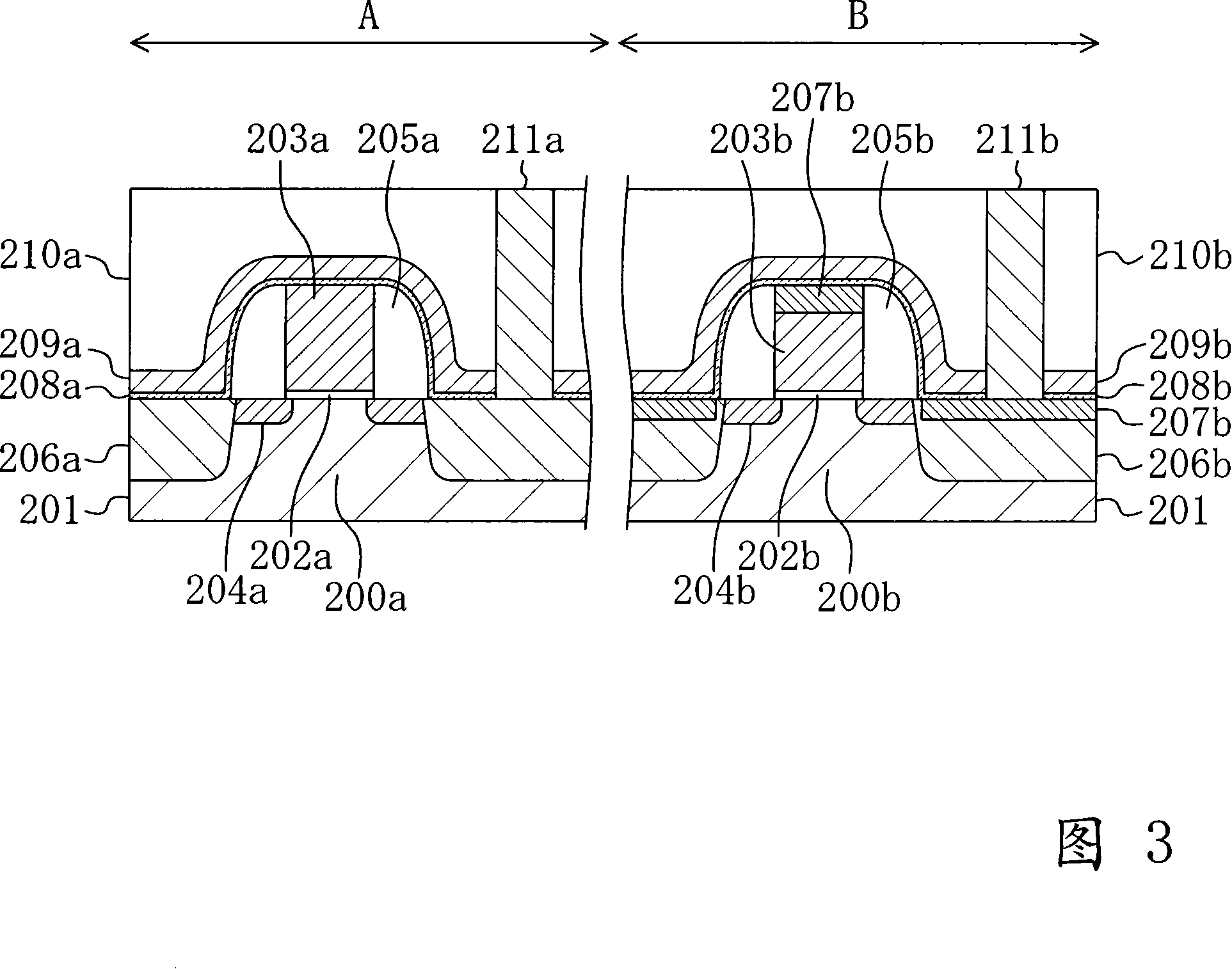
[0092] 3 is a schematic cross-sectional view showing the structure of a semiconductor device according to a second embodiment of the present invention.

[0093] In the region A in which the NMIS transistor is formed shown in FIG. 3 , in the semiconductor substrate 201 made of silicon, for example, an active region surrounded by an element isolation region (not shown) and in which a p-well (not shown) is formed is formed. 200a. On the active region 200a, a gate electrode 203a having a film thickness of approximately 120 nm is formed via a gate insulating film 202a made of, for example, a SiON-based film with a film thickness of approximately 2 nm. In addition, the gate length of the gate electrode 203a is about 50 nm.

[0094] In addition, in the regions on both sides of the gate electrode 203a in the active region ...


PUM


Abstract

The invention discloses a semiconductor device and method for fabricating the same. The semiconductor device has a structure that can eliminate dependency of coating film bottom. The semiconductor device in an active region (100) has a gate insulating film (102), a gate electrode (103), a sidewall (105), a source drain region (106) and a silicide region (107). The semiconductor device also has an underlying insulating film (108) formed over the active region (100) using atomic layer deposition so as to cover the gate electrode (103), the sidewall (105) and the silicide region (107); and a contact liner film (109) formed on the underlying insulating film using plasma CVD and made of a stress insulating film for applying a tensile or compressive stress in a gate length direction in a channel region.

Description

technical field [0001] The present invention relates to a semiconductor device and a manufacturing method thereof, and relates to a field effect transistor including a contact liner film having a uniform film thickness on a wafer surface and a manufacturing method thereof. Background technique [0002] Along with the miniaturization of semiconductor device design rules, the integration level of circuits has increased dramatically, and more than 100 million field-effect metal-insulator-semiconductor (MIS=Metal Insulator Semiconductor) (transistors) are also becoming highly integrated on one chip. Possibility. In order to realize such a chip, not only the development of ultra-fine processing technologies such as lithography and etching, which require processing precision in the order of tens of nanometers, is required, but also in order to ensure the formation of fine transistors. The absolute amount of current is also strongly required to increase the driving force of the tra...

Claims


Application Information

Patent Timeline
Patent Type & Authority Applications(China)
IPC IPC(8): H01L29/78H01L27/088H01L27/092H01L21/336H01L21/31H01L21/318H01L21/8234H01L21/8238
CPCH01L27/092H01L29/7843H01L21/823835H01L21/823871H01L21/823807
Inventor 竹冈慎治
Owner PANASONIC CORP
Why Eureka
Try Eureka