Semiconductor device and its manufacturing method

A manufacturing method and semiconductor technology, applied in semiconductor/solid-state device manufacturing, semiconductor devices, electrical components, etc., can solve problems affecting component performance, short channel effect, electrical breakdown, etc., to improve electrical breakdown effect, suppress The effect of spreading out

Active Publication Date: 2008-09-03
UNITED MICROELECTRONICS CORP
View PDF0 Cites 12 Cited by
  • Summary
  • Abstract
  • Description
  • Claims
  • Application Information

AI Technical Summary

Problems solved by technology

However, the boron doped in the polysilicon germanium layer will inevitably diffuse out
If the boron dopant diffuses vertically, the junction depth will be too deep, which will easily cause problems such as electrical breakdown (punchthrough) effect; if the boron dopant diffuses laterally, it will easily cause short channel effect, which will affect the Component performance

Method used


Image

  • Semiconductor device and its manufacturing method
  • Semiconductor device and its manufacturing method
  • Semiconductor device and its manufacturing method

Examples


Embodiment Construction

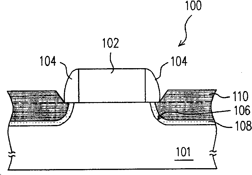
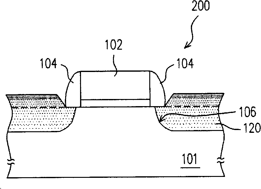
[0029] figure 1 It is a schematic cross-sectional view of a semiconductor device according to an embodiment of the present invention.

[0030] Please refer to figure 1 The semiconductor device 100 of the present invention includes a substrate 101 , a gate structure 102 , a spacer 104 , a first polysilicon germanium layer 108 doped with boron, and a second polysilicon germanium layer 110 . As mentioned above, the substrate 101 is, for example, a silicon substrate or other suitable semiconductor substrate, and has two openings 106 in the substrate 101 . The gate structure 102 is disposed on the substrate 101 between the openings 106, and the gate structure 102 is, for example, composed of a gate dielectric layer (not shown) and a gate conductor layer (not shown), and its material It is well known to those skilled in the art, so details will not be repeated here. In addition, the spacer 104 is disposed on the sidewall of the gate structure 102 and located above the partial ope...


PUM


Abstract

A semiconductor component includes a substrate, a grid structure, a gapping place wall, and a first polysilicon germanium layer with boron dope and a second polysilicon germanium layer. The substrate has two opening, and the grid structure are placed at the substrate between two openings. The gapping wall is configured at the lateral wall of the grid structure, and situated above the two openings. In addition, first polysilicon germanium layer is configured at the surface of the two opening of the substrate, moreover second polysilicon germanium layer is configured at first polysilicon germanium layer, and the top of second polysilicon germanium layer is higher than the surface of the substrate. Wherein, boron concentration of first polysilicon germanium layer is lower than that of second polysilicon germanium layer.

Description

technical field [0001] The invention relates to an element structure of an integrated circuit, and in particular to a semiconductor element and a manufacturing method thereof. Background technique [0002] For silicon metal oxide semiconductor transistor devices, when the gate length is reduced to a deep sub-micron range, better device performance can be obtained because the carrier transit time decreases as the channel length shortens. However, there are still many technical difficulties to be overcome in the development of this kind of process. [0003] At present, in order to obtain better device performance, metal-oxide-semiconductor transistors in which source / drain regions are fabricated by silicon germanium technology are being actively developed. SiGe material can be selectively grown in the source / drain regions, and SiGe material can be selectively etched relative to silicon and silicon oxide. [0004] Usually, a high concentration of boron (boron) is doped into t...

Claims


Application Information

Patent Timeline
Patent Type & Authority Applications(China)
IPC IPC(8): H01L29/78H01L21/336
Inventor 郑博伦
Owner UNITED MICROELECTRONICS CORP
Why Eureka
Try Eureka