A vertical cavity side transmission photon crystal surface wave laser and its design method

A technology of vertical cavity surface emission and photonic crystals, which is applied in the direction of semiconductor lasers, lasers, laser components, etc., can solve the problems of large divergence angle of outgoing laser beams, uneven equi-phase planes, poor directivity, etc., to achieve good directivity, The effect of high quality factor and wide application range

Inactive Publication Date: 2008-09-17
SHANGHAI INST OF MICROSYSTEM & INFORMATION TECH CHINESE ACAD OF SCI
View PDF0 Cites 4 Cited by
  • Summary
  • Abstract
  • Description
  • Claims
  • Application Information

AI Technical Summary

Problems solved by technology

[0007] The surface wave lasers in the prior art belong to the end-emission type. Due to diffraction, the outgoing laser beam has a large divergence angle, so the directivity is poor and the equiphase plane is not flat.

Method used


Image

  • A vertical cavity side transmission photon crystal surface wave laser and its design method
  • A vertical cavity side transmission photon crystal surface wave laser and its design method
  • A vertical cavity side transmission photon crystal surface wave laser and its design method

Examples


Embodiment Construction

[0034] The design method of the vertical cavity surface emitting photonic crystal surface wave laser of the present invention will be described below through two specific embodiments,

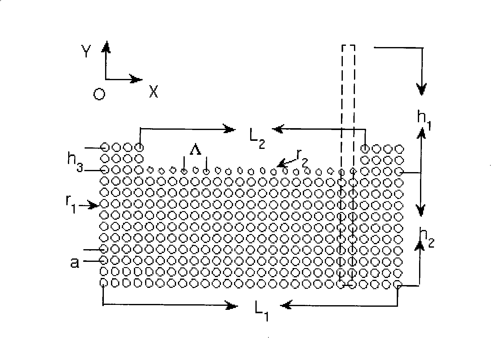
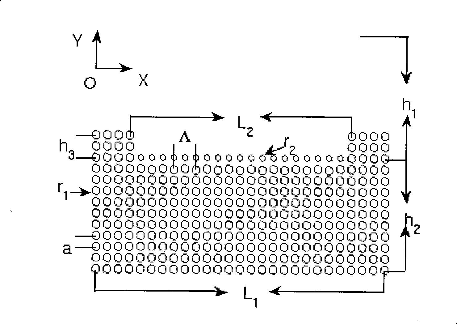
[0035] 1. Select the luminescent material, determine the refractive index of the material, select the photonic crystal structure type, and determine the structural parameters; in the specific embodiment of the present invention, the semiconductor luminescent material InGaAsP is selected, the refractive index is n=3.4, and its center wavelength is 1.55 μm, which is currently The optical communication band is widely used, and the preparation technology of this material is mature. The photonic crystal surface wave cavity (such as figure 1 As shown, the axis of the dielectric column is along the z-axis direction, the surface is along the x-axis direction, and the y-axis is perpendicular to the cavity surface): the cavity is a two-dimensional square lattice structure composed of multiple dielectric ...


PUM


Abstract

The present invention provides a vertical cavity surface emitting photonic crystal surface wave laser and its design method, the design method includes following steps: step 1: choosing a luminescent material, determining the material refractive index, selecting structure model of the photonic crystal, determining the structure parameter; step 2. calculating the dispersion relation of the structure by the super cell technology and the plane wave expansion method, obtaining a surface model; step 3. planning a surface wave micro-cavity body, the surface layer of the cavity body has periodic undulation. The invention properly changes the surface layer structure of the photonic crystal, the surface layer or the adjacent layer of the surface layer has periodic undulation, so as to improve the emitting direction of the surface wave laser, changing to a vertical cavity surface emission from the original end emission, and the constant phase surface of the emission is very flat. The design of the invention has simple thinking, better integrity, widely applying range, designing the surface wave laser of different wave bands according to the luminescent characteristic of the different materials, especially designing light source device of the light communication wave band using semiconductor material having important value.

Description

technical field [0001] The invention provides a vertical cavity surface-emitting photonic crystal surface wave laser and a design method thereof, belonging to the technical fields of optoelectronics, optical communication, and the like. Background technique [0002] Photonic crystals are dielectric materials whose refractive index changes periodically in space, which can effectively control the propagation behavior of photons. Since E. Yablonovitch and S. John proposed this concept twenty years ago, people have paid extensive attention to the application of photonic crystals. Especially in the field of optical communication technology, photonic crystal devices such as photonic crystal fibers, microresonator lasers, filters, and integrated optical circuits have broad application prospects. The continuous improvement of semiconductor material microfabrication technology has greatly promoted the application of two-dimensional and even three-dimensional photonic crystal devices...

Claims


Application Information

Patent Timeline
Patent Type & Authority Applications(China)
IPC IPC(8): H01S5/183
Inventor 蒋寻涯赵德印周传宏张永亮
Owner SHANGHAI INST OF MICROSYSTEM & INFORMATION TECH CHINESE ACAD OF SCI
Why Eureka
Try Eureka