
Laser processing device, positioning device; observing device and observing method

An observation device and laser processing technology, applied in metal processing equipment, laser welding equipment, manufacturing tools, etc., can solve the problems of unstable segmentation position determination accuracy and uneven transmittance.

Active Publication Date: 2011-04-06
MITSUBOSHI DIAMOND IND CO LTD
View PDF1 Cites 0 Cited by
  • Summary
  • Abstract
  • Description
  • Claims
  • Application Information

AI Technical Summary

Problems solved by technology

[0013] And in the case of such transmitted illumination, due to the unevenness of the transmittance between the substrates (lots), and the contrast (the sharpness of the image of the device pattern observed and captured) when observing the device pattern different transparent substrates, resulting in unstable determination accuracy of the segmentation position

Method used


Image

  • Laser processing device, positioning device; observing device and observing method
  • Laser processing device, positioning device; observing device and observing method
  • Laser processing device, positioning device; observing device and observing method

Examples


no. 1 approach

[0054]

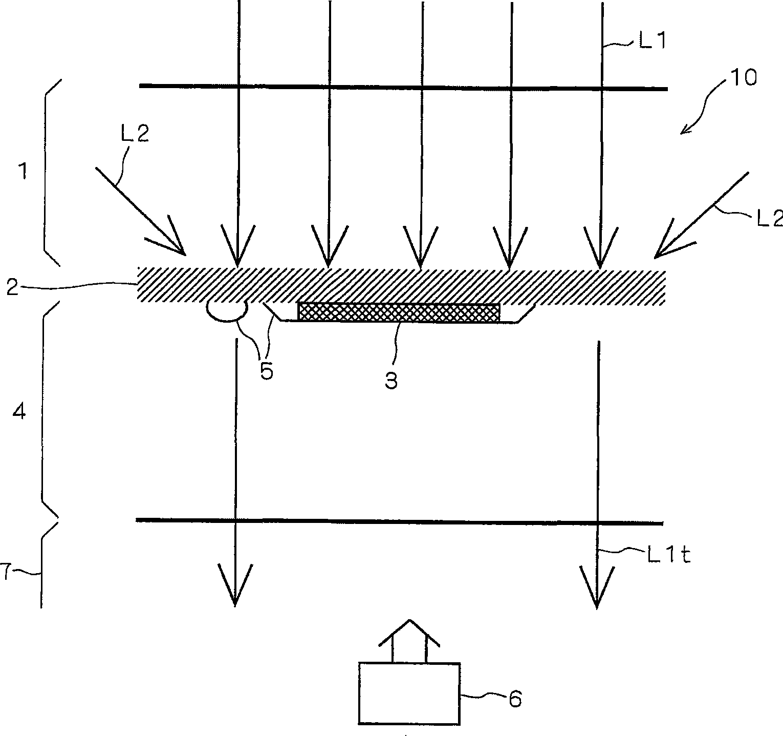
[0055] Figure 1A , Figure 1B It is used to describe the observation method of the first embodiment of the present invention. In this embodiment, the observation objects are as Figure 1A Shown is a laminate 10 in which a diffusion layer 2 for diffusing illumination light for observation is provided as a base layer on one main surface of a transparent substrate 1 such as sapphire, and an opaque device pattern 3 such as metal wiring and electrodes is formed. , as an example.

[0056] Alternatively, a transparent semiconductor layer made of a Group III nitride such as GaN (gallium nitride) may be provided between the transparent substrate 1 and the device pattern 3 .

[0057] In addition, in this embodiment, if Figure 1A As shown, an adhesive sheet 4 is pasted on the main surface of the laminated body 10 on which the device pattern 3 is formed, and the adhesive sheet 4 side is fixed to a transparent carrier 7 made of, for example, quartz to perform device patter...

no. 2 approach

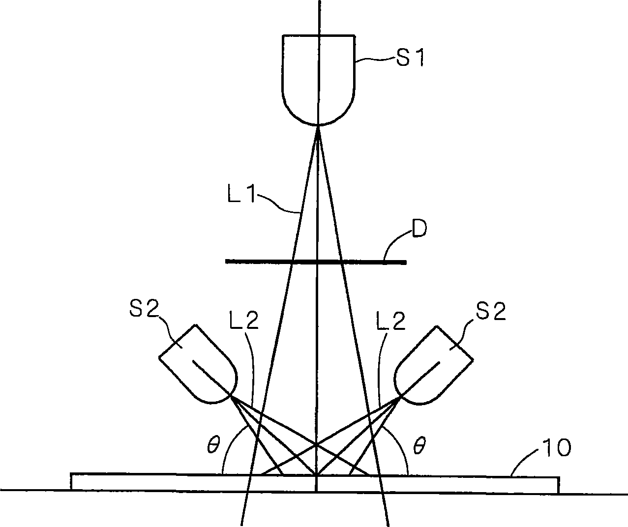
[0088] In the above-mentioned embodiment, the case where the laminated body 10 is observed in a state where, for example, the back surface observation unit 50B of the laser processing apparatus 50 is simultaneously irradiated with the coaxial illumination light L1 having an incident angle of 90 degrees and the incident angle This is the case of oblique illumination light L2 at an acute angle, but of course the observation method is not limited to this.

[0089] FIG. 4 is a schematic configuration diagram schematically showing a laser processing apparatus 500 according to a second embodiment. In addition, the same reference numerals are assigned to the same configurations as those of the laser processing apparatus 50 of the first embodiment, and explanations thereof are appropriately omitted.

[0090] The laser processing apparatus 500 is equipped with the control part C comprised from an ordinary computer etc.. As shown in FIG. The control unit C is connected to each mechanis...


PUM


Abstract

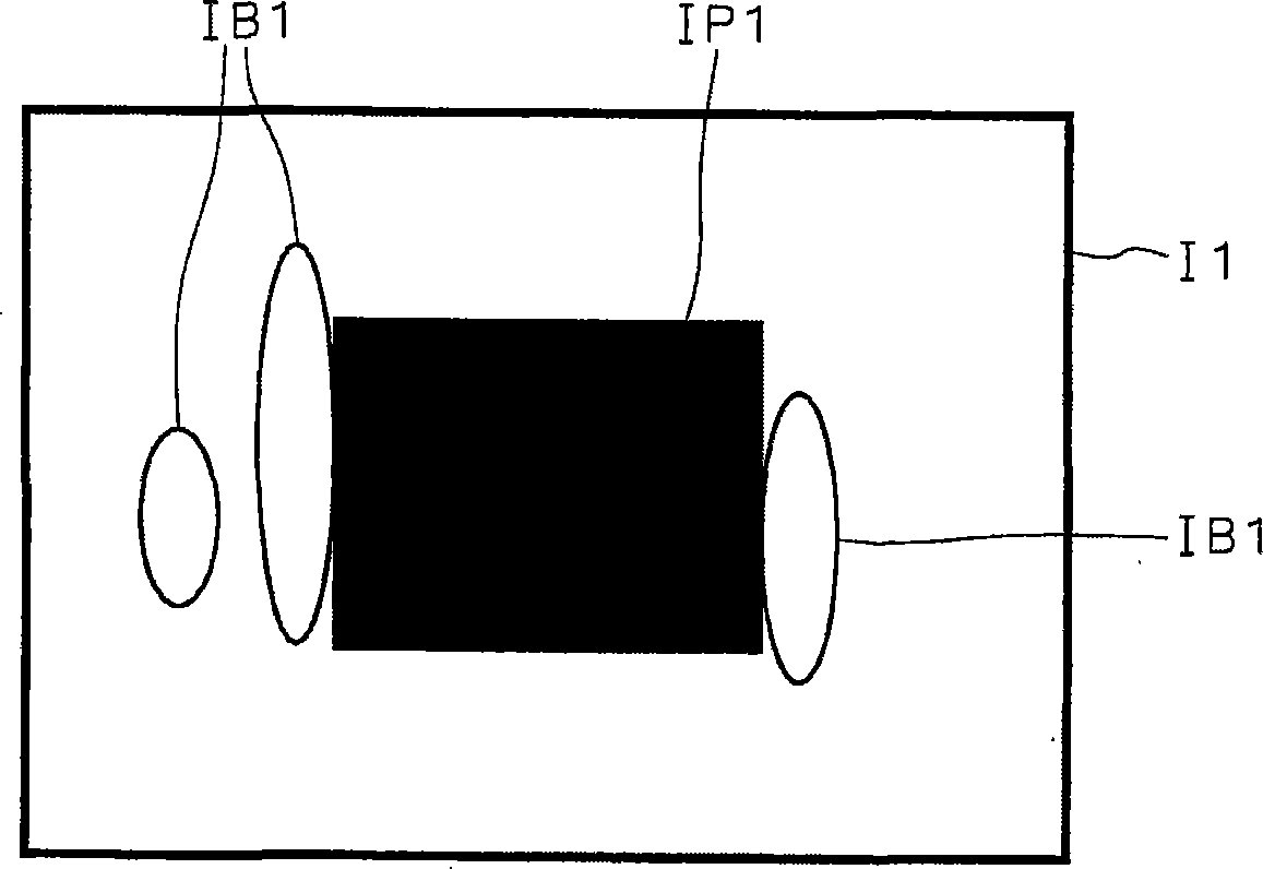
An observation method and an observation device capable of definitely identifying an opaque device pattern formed on a transparent substrate in an observation image d are provided. A bonding plate (4) is bonded to one side formed with the device pattern (3), the transparent substrate is fixed at a transparent carrying table (7) above which an axial transmission irradiation light (L1) and an inclined transmission irradiation light (L2) irradiate in an overlap manner, and the observation is performed via the carrying table (7) by using a back observation unit (6) from the lower direction of thecarrying table (7); in the observation image, the dark (black) device pattern images and the bright part other than the device pattern images are observed corresponding to the device pattern (3). Furthermore, the part corresponding to bubbles are quite bright such that the shape of the device pattern (3) can be definitely determined in the observation image.

Description

technical field [0001] The present invention relates to a technology capable of clearly recognizing a device pattern provided on a transparent or translucent substrate by observing an image. Background technique [0002] A method is known in which, in order to form a device pattern such as a short-wavelength LD (laser diode) or LED (light-emitting diode) on a substrate using a brittle material with high hardness such as sapphire, a method is known in which a pulsed laser beam is irradiated to form a pattern for division. The starting point method (for example, refer to Patent Document 1). [0003] When using the device disclosed in Patent Document 1 or other devices to form a starting point for dividing the substrate into device chip units, an observation optical system composed of a CCD (Charge coupled device) camera or the like is used to observe the Observation and imaging are carried out with the specified position reference object, and based on the obtained imaging dat...

Claims


Application Information

Patent Timeline
Patent Type & Authority Patents(China)
IPC IPC(8): B23K26/03B23K26/02B23K26/40
Inventor 小川纯一栗山规由林和夫庭山博
Owner MITSUBOSHI DIAMOND IND CO LTD
Learn More