Method for preparing thin-film transistor array substrate and liquid crystal display panel

A technology of thin film transistors and array substrates, which is applied in the field of manufacturing thin film transistor array substrates, can solve problems such as reduction, insufficient polysilicon film thickness, and distortion of measurement results, so as to increase the photosensitive area, improve light sensing performance, and avoid noise influence Effect

Inactive Publication Date: 2008-10-01
AU OPTRONICS CORP
View PDF0 Cites 22 Cited by
  • Summary
  • Abstract
  • Description
  • Claims
  • Application Information

AI Technical Summary

Problems solved by technology

However, due to process limitations, the p-i-n photosensor manufactured by LTPS technology will cause poor quantum effect (Quantum Effect, that is, photoelectric conversion efficiency) due to insufficient polysilicon film thickness.
In addition, the light emitted by the backlight will directly irradiate the p-i-n light sensor through the glass substrate, which will affect the light-sensing characteristics of the p-i-n light sensor, reducing the signal-to-noise ratio (SNR) of the light-sensing signal, resulting in distortion of the measurement results

Method used


Image

  • Method for preparing thin-film transistor array substrate and liquid crystal display panel
  • Method for preparing thin-film transistor array substrate and liquid crystal display panel
  • Method for preparing thin-film transistor array substrate and liquid crystal display panel

Examples


Embodiment Construction

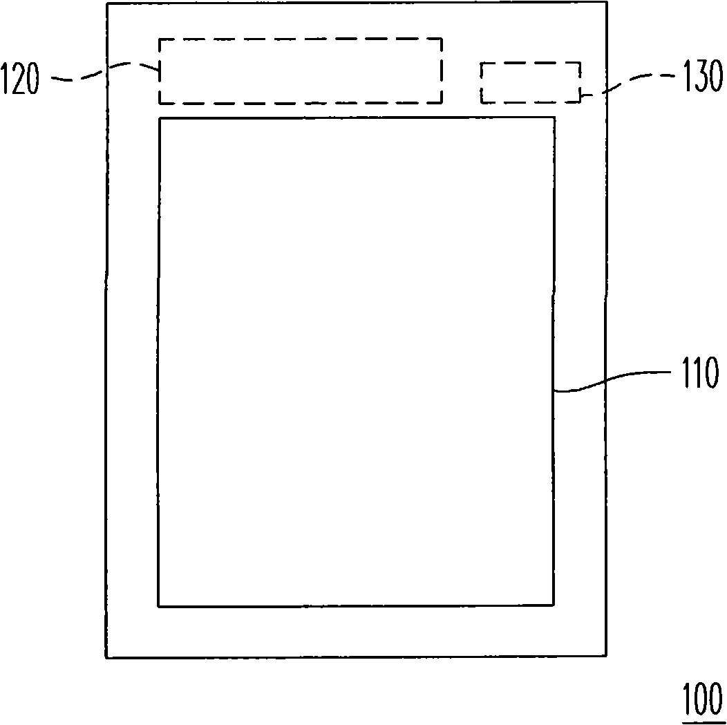
[0110] Please refer to figure 1 , which shows a layout of a liquid crystal display panel integrated with light sensors according to an embodiment of the present invention. like figure 1 As shown, the liquid crystal display panel 100 has at least a display area 110 and a peripheral circuit area 120 and a sensing area 130 located on the periphery of the display area 110 . There are a plurality of pixel units in the display area 110 to display a picture frame. Possible driving components, such as a scan driver or a data driver, are arranged in the peripheral circuit area 120 . The sensing area 130 is used to configure a light sensor to detect the intensity of ambient light, and accordingly adjust the brightness of the back-light of the display to achieve the effect of power saving. At the same time, by detecting the intensity of ambient light, the brightness and contrast of the liquid crystal display panel can also be automatically adjusted, which can not only alleviate eye fa...


PUM


Abstract

The invention discloses a method for manufacturing thin film transistor array substrate and liquid crystal display panel, the method for manufacturing thin film transistor array substrate integrates the manufacturing of an optical sensor, a photosensitive dielectric layer is formed between a transparent conductive layer and a metal electrode to sense the external light. As the optical sensor uses the transparent conductive layer as an electrode, the external light can directly irradiate the photosensitive dielectric layer through the transparent conductive layer, dramatically increasing the sensitization area of the optical sensor and promoting the light sensing performance. In addition, another side of the photosensitive dielectric layer is metal electrode, therefore efficiently preventing the backlight from directly irradiating the photosensitive dielectric layer and avoiding the noise.

Description

technical field [0001] The present invention relates to a manufacturing method of a thin film transistor array substrate, and in particular to a manufacturing method of a thin film transistor array substrate integrated with a light sensor. Background technique [0002] With the popularity of liquid crystal and plasma displays, flat panel displays have become so-called "Multimedia Boards" in addition to viewing images. The ambient light (Ambient Light) sensing function integrated in the flat panel display is a new proposal of current display technology, which mainly builds a light sensor in the flat panel display to detect the intensity of ambient light. [0003] The current common ambient light sensing technology is to form p-i-n (positively doped / undoped / negatively doped) photosensors on the glass substrate of the display panel by Low Temperature Poly-Silicon (LTPS) process. However, due to process limitations, the p-i-n photosensor manufactured by LTPS technology will suf...

Claims


Application Information

Patent Timeline
Patent Type & Authority Applications(China)
IPC IPC(8): H01L21/84H01L21/768H01L27/144H01L23/522G02F1/1333G02F1/1362
Inventor 卓恩宗彭佳添翁健森林昆志曾泓玮庄铭宏
Owner AU OPTRONICS CORP
Why Eureka
Try Eureka