Multilayer printed wiring board

A multi-layer printing and circuit board technology, applied in the direction of printed circuit, printed circuit, printed circuit manufacturing, etc., can solve the problem of IC chip malfunction, and achieve the effect of causing malfunction, reducing mutual inductance, and suppressing the delay of power supply.

Active Publication Date: 2008-10-01
IBIDEN CO LTD
View PDF1 Cites 11 Cited by
  • Summary
  • Abstract
  • Description
  • Claims
  • Application Information

AI Technical Summary

Problems solved by technology

[0003] In the above-mentioned multilayer printed circuit board for semiconductor element mounting in the prior art, there is the following problem: the high-speed cir

Method used


Image

  • Multilayer printed wiring board
  • Multilayer printed wiring board
  • Multilayer printed wiring board

Examples


Embodiment 1

[0059] A. Preparation of resin composition for through-hole filling

[0060] By coating 100 parts by weight of bisphenol F-type epoxy monomer (manufactured by Yukashiel Co., molecular weight: 310, YL983U) on the surface, the average particle size of the silane coupling agent is 1.6 μm, and the maximum particle size is 15 μm or less. SiO 2 170 parts by weight of spherical particles (manufactured by Adotec, CRS 1101-CE) and 1.5 parts by weight of a leveling agent (manufactured by Sannopuko, Perenoru S4) were placed in a container, stirred and mixed to prepare It is a resin filling material whose viscosity is 44-49 Pa·s at 23±1°C. In addition, as a curing agent, 6.5 parts by weight of an imidazole curing agent (manufactured by Shikoku Chemicals Co., Ltd., 2E4MZ-CN) was used. As the resin for filling the through-holes, other thermosetting resins such as epoxy resins (for example, bisphenol F type and phenolic resin types), polyimide resins, and phenolic resins may be used. The ...

Embodiment 2

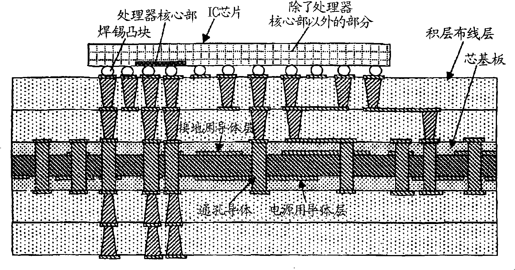
[0128] In the step (5) of Example 1, the pitch for forming via-hole conductors was changed. Via-hole conductors are not formed directly under all pads directly under the processor core portion 80a (via-hole conductors can be formed within a range of 50 to 100% of the number of pads directly under the processor core portion), but The via-hole conductors are formed every other land, and therefore, the pitch is 250 μm. Via-hole conductors are formed at a pitch of 300 to 600 μm to account for 10% of the number of pads except directly below the processor core 80 a in the region other than directly below the processor core 80 a. Except for this, a multilayer printed wiring board was produced in the same manner as in Example 1.

Embodiment 3

[0130] In step (5) of Example 1, the number of through-holes for forming via-hole conductors was changed. Directly below the processor core unit 80a is the same as that of the first embodiment. In the region other than directly under the processor core part, 50% of via conductors are formed with respect to the number of pads except directly under the processor core part 80a. Immediately below the IC chip 80, directly under the portion 80b other than the processor core portion 80a, via-hole conductors are formed at a pitch of 150 to 400 μm, and at the portion other than the IC chip 80, formed at a pitch of 300 to 600 μm. The spacing forms via conductors. Except for this, a multilayer printed wiring board was produced in the same manner as in Example 1.


PUM

PropertyMeasurementUnit
Diameteraaaaaaaaaa
Thicknessaaaaaaaaaa
Current densityaaaaaaaaaa

Abstract

A multilayer printed wiring board has a mounting section for mounting a semiconductor element such as an IC chip on a surface layer of a build up wiring layer. The pitch of a through hole conductors arranged in regions directly below regions whereupon semiconductor elements such as IC chips are mounted is permitted to be smaller than that of through hole conductors arranged in other regions. Thus, delay of power supply to the transistor of the processor core section of the mounted IC chip is suppressed and malfunctioning is prevented from being easily generated.

Description

technical field [0001] The present invention relates to a multilayer printed wiring board on which semiconductor elements such as IC chips are mounted, and more particularly to a semiconductor element mounting substrate capable of suppressing malfunctions in high-frequency regions. Background technique [0002] As a conventional semiconductor element mounting substrate, there is a build-up substrate in which insulating layers and conductor circuits are alternately laminated on a core substrate on which via-hole conductors are formed (see JP 2002-374066 ). [0003] In the multilayer printed wiring board for mounting semiconductor elements in the prior art, there is a problem that when an IC chip driven at a high speed of 3 GHz or higher and having a large size and a large number of electrodes is mounted on a substrate, the IC chip after mounting will be damaged. Misoperation is prone to occur. Contents of the invention [0004] Accordingly, an object of the present inventi...

Claims


Application Information

Patent Timeline
IPC IPC(8): H01L23/12H05K3/46
CPCH01L2224/16225H01L23/49816H01L23/49827H05K1/115H01L23/49822H05K2201/10674H05K3/4602H01L2224/16227H01L23/49838H05K2201/0352H05K2201/09536H05K2201/096H05K3/4652H05K1/113Y10T29/49139H01L23/12H05K3/46
Inventor 苅谷隆
Owner IBIDEN CO LTD
Why Eureka
Try Eureka