
Printed circuit board and producing method of encapsulation base of integrated circuit

一种印制电路板、集成电路的技术,应用在印刷电路制造、印刷电路、印刷电路等方向,能够解决不利精细线路、线路铜厚厚、限制半加成法应用等问题,达到降低的困难、增加布线密度、避免成本较高的效果

Active Publication Date: 2008-10-15
SHANGHAI MEADVILLE SCI & TECH
View PDF0 Cites 45 Cited by
  • Summary
  • Abstract
  • Description
  • Claims
  • Application Information

AI Technical Summary

Problems solved by technology

However, in the actual electroplating process, the copper thickness of the line is generally too thick to fill the blind hole, which is not conducive to the production of fine lines.
[0011] To sum up, the semi-additive method can realize the production of fine lines, and has become the preferred process for the production of fine lines, but the ordinary semi-additive method cannot solve the problem of how to form solid conductive vias, and then stack holes to achieve any layer connection. Therefore, the application of the semi-additive method is greatly limited.

Method used


Image

  • Printed circuit board and producing method of encapsulation base of integrated circuit
  • Printed circuit board and producing method of encapsulation base of integrated circuit
  • Printed circuit board and producing method of encapsulation base of integrated circuit

Examples


Embodiment Construction

[0033] The manufacturing method of the present invention will be further described below in conjunction with the accompanying drawings.

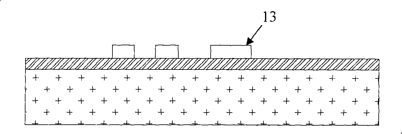
[0034] Such as Figure 6a , Figure 6b , Figure 6c , Figure 6d , Figure 6e , Figure 6f , Figure 6g , Figure 6h , Figure 6i , Figure 6j As shown (in the figure, 61 is the bottom dielectric layer, 62 is the copper foil, 63 is the dielectric layer, 64 is the first seed layer, 65 is the copper layer, 66 is the second seed layer, and 67 is the anti-plating layer), the concrete made by the present invention The steps are:

[0035] step 1( Figure 6a ), first fabricate a dielectric layer 63 on the substrate: in this embodiment, the substrate is a composite material of a bottom dielectric layer 61 and a layer of copper foil 62 . The dielectric layer can be fabricated on the substrate by resin coating, film sticking, or lamination of the dielectric layer. If lamination is used, the laminate dielectric layer may or may not be cover...


PUM


Abstract

The invention relates to a manufacturing method of a printed circuit board and an integrated circuit packaging substrate; based on the interconnection of electroplating pore filling and a semi-additive forming layer and a fine circuit, the method comprises the following steps: (1) a dielectric layer is manufactured on the substrate; (2) blind hole structure is manufactured on the dielectric layer; (3) after the blind hole structure is completed, a first conductive seed layer is manufactured; (4) a solid conductive via hole is manufactured by adopting the method of electroplating pore filling, and a copper layer grows and covers on the first seed layer in the process of electroplating pore filling; (5) the copper layer and the first seed layer are removed, and a solid copper cylinder in the solid conductive via hole is retained; (6) a second seed layer of semi-additive manufacturing circuit is manufactured; (7) a photosensitive thin film is glued, an anti-plating layer is formed by transferring diagram and the circuit diagram is exposed: (8) the circuit in the circuit diagram is thickened; (9) the photosensitive thin film and the exposed second seed layer are removed, the thickened circuit is retained, and a needed conductive diagram is formed; (10) all the steps from (1) to (9) are repeated on the new circuit surface, and the manufacture of fine circuits of following circuit layers and the connection of the solid conductive via holes in the layers are completed.

Description

technical field [0001] The invention relates to a semi-additive manufacturing technology for printed circuit boards and semiconductor integrated circuit packaging substrates, in particular to a manufacturing method for realizing interlayer interconnection based on electroplating hole-filling technology and using a semi-additive method to manufacture fine circuits. Background technique [0002] With the development of society and science and technology, electronic products are increasingly miniaturized. This development trend has also led to the development of printed circuit boards for connecting different devices and substrates for semiconductor chip packaging under the premise of ensuring good electrical and thermal properties. Develop in the direction of light, thin, short and small. In order to meet the above requirements, smaller fine lines and smaller high-reliability conductive vias are two technical requirements that must be met at the same time. [0003] According ...

Claims


Application Information

Patent Timeline
Patent Type & Authority Applications(China)
IPC IPC(8): H01L21/48H05K3/46
CPCH05K3/4644H05K3/108H05K3/421H05K2201/09563H05K2203/025H05K2203/1476
Inventor 程凡雄陈培峰付海涛罗永红
Owner SHANGHAI MEADVILLE SCI & TECH
Learn More