Process for manufacturing three-dimensional miniature mold

A manufacturing method and miniature technology, which is applied in the field of mold manufacturing, can solve the problems of large mold cavity size, small micro mold depth and width, complex processing technology, etc., and achieve the effects of high precision, low cost and large process flexibility

Inactive Publication Date: 2008-10-29
HUAZHONG UNIV OF SCI & TECH
View PDF0 Cites 3 Cited by
  • Summary
  • Abstract
  • Description
  • Claims
  • Application Information

AI Technical Summary

Problems solved by technology

Micro special processing techniques such as electrochemistry are relatively complex, and have irreplaceable advantages in the processing of mold cavities for difficult-to-cut materials, complex profiles, and low-rigidity materials, but there are still deficiencies in the processing of three-dimensional micro-part molds; laser processing It mainly includes excimer laser processing and femtosecond laser processing. Due to the limitation of laser focusing, the processed micro-molds have a relatively small aspect ratio; the traditional micro-machining method to process three-dimensional micro-mold cavities, although the process is simple and practical, is not It can be produced with too much investment, but the cavity size of the processing mold is large and the precision is low

Method used


Image

  • Process for manufacturing three-dimensional miniature mold
  • Process for manufacturing three-dimensional miniature mold
  • Process for manufacturing three-dimensional miniature mold

Examples


Embodiment 1

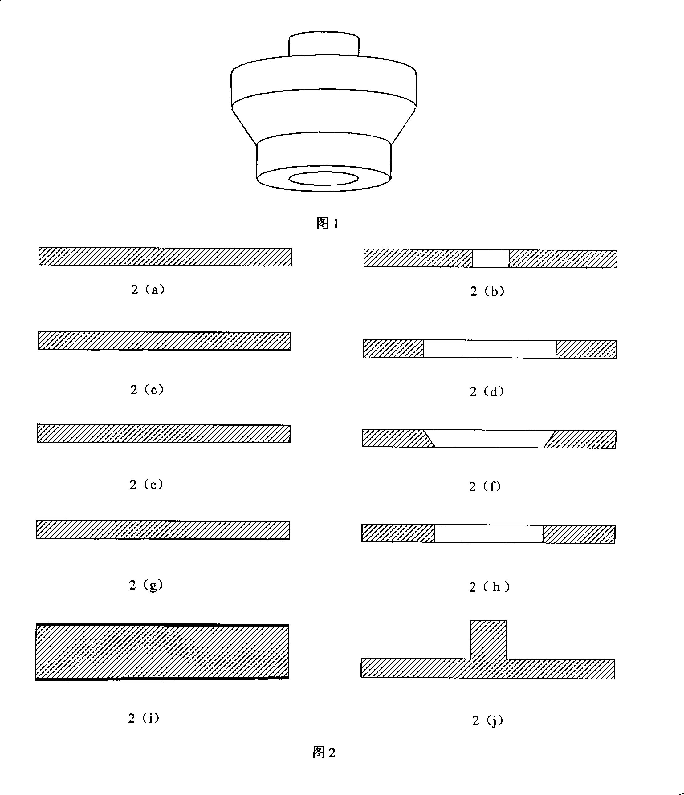
[0023] Fig. 1 shows the three-dimensional micro-parts to be manufactured aimed at the mold made by the present embodiment, the part is divided into 5 layers in the vertical direction, 5 standard silicon wafers are selected, and the silicon wafers are thinned, Fig. 2(a) , Figure 2(c), Figure 2(e) and Figure 2(g) show the thickness of the silicon wafer is 100μm, the thickness of the silicon wafer shown in Figure 2(i) is 300μm, adopt bulk silicon processing technology on the silicon wafer The appearance patterns of each layer of the part are etched in sequence, as shown in Figure 2(b), Figure 2(d), Figure 2(f), Figure 2(h) and Figure 2(j), Figure 2(j) The silicon wafer is etched with the appearance shape of the bottom layer of the part.

[0024] Soak the etched sample to be bonded in the cleaning solution (H 2 SO 4 :H 2 o 2 = 2:1), wash at 120°C for 20 minutes;

[0025] Soak the cleaned silicon wafer in ammonia activation solution (NH 4 OH:H 2 o 2 :H 2 (0=1:1:5) was acti...

Embodiment 2

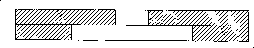
[0030] Figure 5 For the parts that the mold made in this embodiment is aimed at, the mold is divided into three layers, the preparation steps are roughly the same as in Example 1, the difference is: (1) using H 2 SO 4 :H 2 o 2 =4:1 cleaning solution for 15 minutes; (2) using 70% HNO 3 Activation is carried out, the activation time is 20 minutes, and the reaction temperature is 70°C; (3) Lamination is carried out in the order from bottom to top; (4) The annealing time is 10 hours, and the annealing temperature is 450°C. Figure 6 It is a schematic diagram of the cross-sectional effect of the mold manufactured in this embodiment.

Embodiment 3

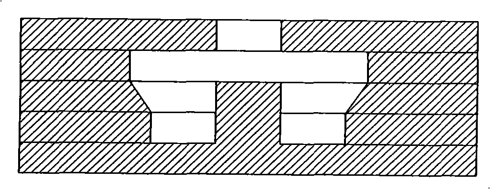
[0032] Figure 7 The part for which the mold made in this embodiment can be divided into three layers from a structural point of view, but because the two ends of the micro part have a relatively high aspect ratio, when the existing etching technology cannot be etched through, It is divided into two layers, so this part is divided into five layers, the mold preparation steps are roughly the same as in Example 1, the difference is: (1) using H 2 SO 4 :H 2 o 2 = 3:1 cleaning solution, cleaning at 120°C for 10 minutes; (2) using 70% HNO 3 Activation is carried out, the activation time is 20 minutes, and the reaction temperature is 70°C; (3) Lamination is carried out in the order from bottom to top; (4) The annealing time is 8 hours, and the annealing temperature is 500°C. Figure 8 It is a schematic diagram of the cross-sectional effect of the mold manufactured in this embodiment.

[0033] In the specific implementation of the present invention, each silicon chip can be thin...


PUM

PropertyMeasurementUnit
thicknessaaaaaaaaaa
thicknessaaaaaaaaaa
thicknessaaaaaaaaaa

Abstract

The invention provides a method for manufacturing a three-dimensional minitype die; patterns corresponding to each layer structure of the parts to be manufactured are respectively etched on each silicon wafer; H2SO4 with the weight percentage of 98% and H2O2 with the weight percentage of 98% are mixed by the volume ratio of 2-4:1; the mixed solution is then used for cleaning all silicon wafers; the silicon wafers are then activated and dried; the silicon wafers are then rapidly aligned and bonded by layer; finally, the three-dimensional die cavity is gained by the annealing disposal. The method of the invention can manufacture the three-dimensional minitype die with micron meter dimension, has the advantages of high precision, low cost and large flexibility and is applicable to the processing and manufacture of micro electro-mechanical system device dies such as micro-gear shafts, micro-step shafts and high depth-width-ratio three-dimensional minitype structure, etc.

Description

technical field [0001] The invention relates to mold manufacturing technology, in particular to a manufacturing method of a three-dimensional miniature mold. Background technique [0002] In the existing technology, the feature size of the part size is between 1 μm and 10 mm, which is called micro parts. With the increasing application of micro parts, especially the rapid development of micro-electromechanical systems (MEMS), electronic industry and other fields, making micro parts Mold manufacturing and micro-forming technology have become the focus of research in the industry. [0003] At present, the micro-machining technology of micro-mold mainly includes electrochemical micro-machining, laser processing technology and precision machining based on metal or non-metal, such as micro-turning, grinding and milling processes. Micro special processing techniques such as electrochemistry are relatively complex, and have irreplaceable advantages in the processing of mold caviti...

Claims


Application Information

Patent Timeline
Patent Type & Authority Applications(China)
IPC IPC(8): B81C5/00B81C99/00
Inventor 史铁林廖广兰王栋聂磊汤自荣彭平阮传值
Owner HUAZHONG UNIV OF SCI & TECH
Why Eureka
Try Eureka