Lithography system, sensor and measuring method

A lithography system and sensor technology, applied in discharge tubes, electrical components, circuits, etc., can solve the problems of known systems such as expensiveness, inability to calibrate charged particle beams, etc., and achieve high pixel resolution and low cost.

Inactive Publication Date: 2008-11-05
MAPPER LITHOGRAPHY IP
View PDF2 Cites 22 Cited by
  • Summary
  • Abstract
  • Description
  • Claims
  • Application Information

AI Technical Summary

Problems solved by technology

In addition to the above-mentioned volumetric characteristics of the known sensor and calibration system, this known system is relatively expensive and moreover cannot calibrate a large number of charged particle beams in a qualitative and sufficiently rapid manner
[0011] In a large number of multi-beam lithography systems, other issues arise, such as adjacent beams should not affect the accuracy of position detection
Also, the known methods and systems do not clarify how to perform data acquisition and data processing for all of the large number of write beams in a reasonably defined time, i.e., in a time period much smaller than the time required to write to a wafer

Method used


Image

  • Lithography system, sensor and measuring method
  • Lithography system, sensor and measuring method
  • Lithography system, sensor and measuring method

Examples


Embodiment Construction

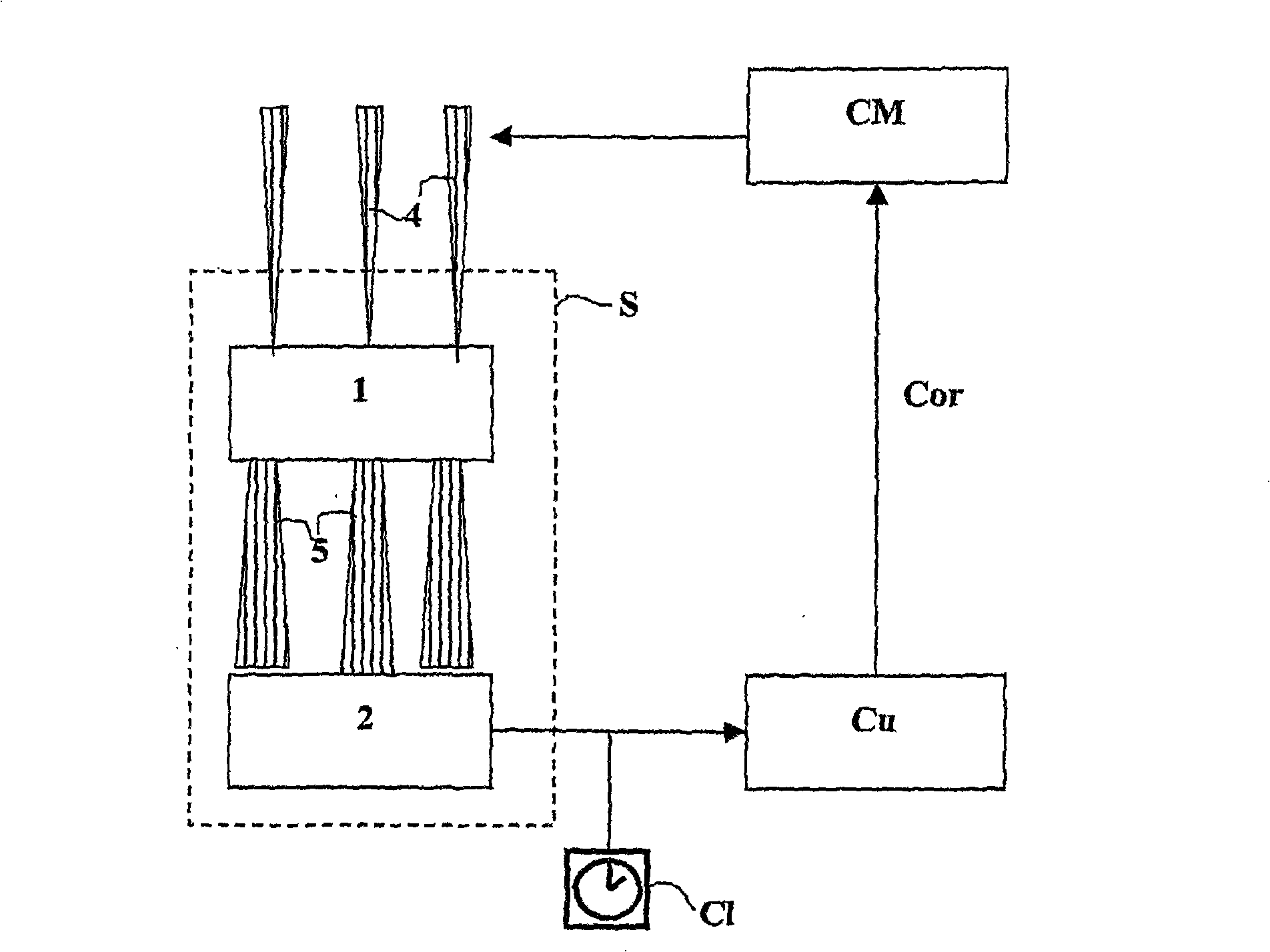
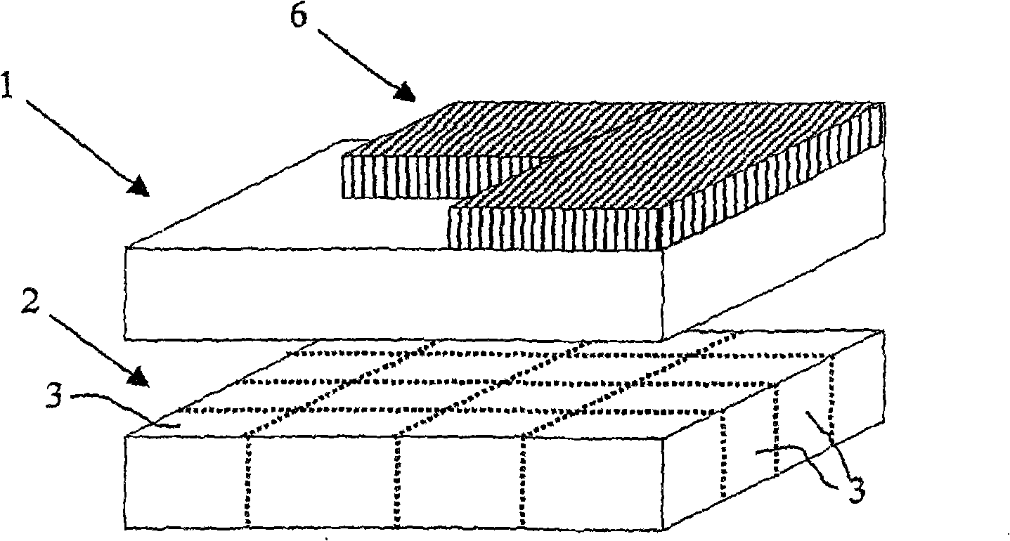
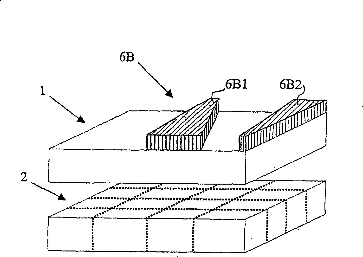
[0042] The present invention provides a design for a lithography system provided with an e-beam alignment sensor suitable for delivering patterns at existing requirements (e.g. 45nm and smaller at speeds of 10 wafers per hour or more) (electron beam alignment sensor). The present invention consists of a new sensor for detecting emitted charged particles in a lithographic system known per se (for example in WO 04 / 038509 in the name of the applicant) or in a multi-beam detection tool Properties of beams such as electron beams. The new sensor consists of a scintillator, here in the form of a so-called YAG (Yttrium Aluminum Garnet) material, combined with a CCD (Charge Coupled Device), denoted alternatively as a camera. The YAG screen used here is Ce (cerium) doped garnet. The characteristics of the charged particle beam are obtained by automatic electronic detection and calculation means from the measurement of the signal generated when the charged particle beam is moved relati...


PUM


Abstract

Lithography system, sensor and method for measuring properties of a massive amount of charged particle beams of a charged particle beam system, in particular a direct write lithography system, in which the charged particle beams are converted into light beams by using a converter element, using an array of light sensitive detectors such as diodes, CCD or CMOS devices, located in line with said converter element, for detecting said light beams, electronically reading out resulting signals from said detectors after exposure thereof by said light beams, utilising said signals for determining values for one or more beam properties, thereby using an automated electronic calculator, and electronically adapting the charged particle system so as to correct for out of specification range values for all or a number of said charged particle beams, each for one or more properties,; based on said calculated property values.

Description

technical field [0001] The invention relates to a multiple particle beam lithography system, a sensor and a method for said system. Such lithographic systems generally operate according to a method for transferring a pattern to a target surface, usually using a so-called particle beam tool for generating said mass of charged particle beamlets, which by means of electronic control The beam may be scanned in one or more directions. A large number of beamlets (also denoted writing beam) will hereinafter be calibrated through the sensor. Such lithographic systems are usually based on a method comprising the steps of generating a plurality of writing beams for writing said pattern on said target surface, usually a wafer or a mask. Preferably, the writing beam may consist of an electron beam emitted by a writing beam source, which may for example comprise a cathode, and which may be appended with a writing beam shaping device, such as an array of apertures, for converting the beam...

Claims


Application Information

Patent Timeline
Patent Type & Authority Applications(China)
IPC IPC(8): H01J37/317
Inventor 彼得·克勒伊特马尔科·扬·哈科·威兰埃尔温·斯洛特蒂斯·弗兰斯·泰佩恩斯泰恩·威廉·卡雷尔·赫尔曼·斯腾布林克
Owner MAPPER LITHOGRAPHY IP
Why Eureka
Try Eureka