Method for forming CMOS image sensor
A technology of image sensor and MOS transistor, which is applied in semiconductor/solid-state device manufacturing, electrical components, circuits, etc., can solve the problems of increasing dark current and photodiode without protective layer, so as to reduce dark current and prevent contamination Effect
- Summary
- Abstract
- Description
- Claims
- Application Information
AI Technical Summary
Problems solved by technology
Method used
Image

Examples
Embodiment Construction
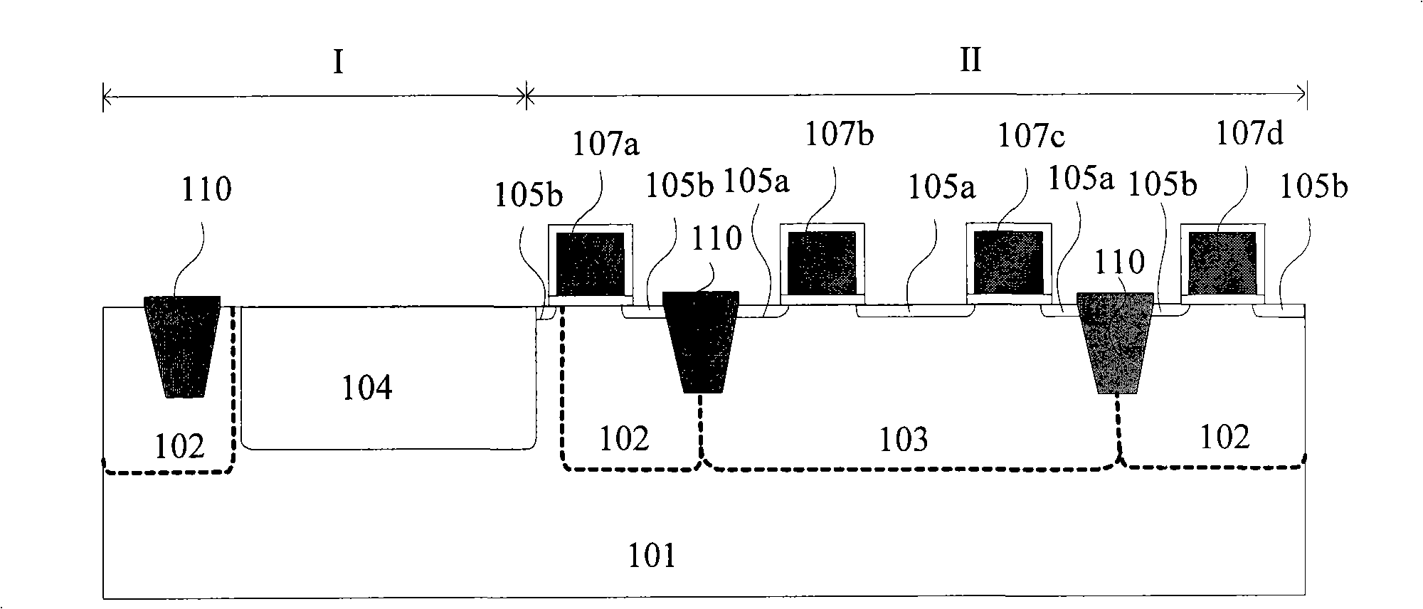
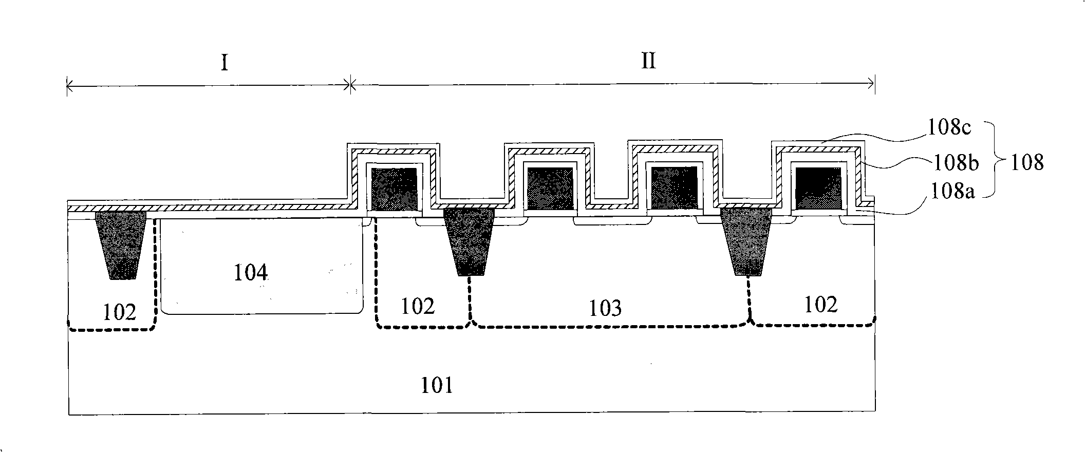
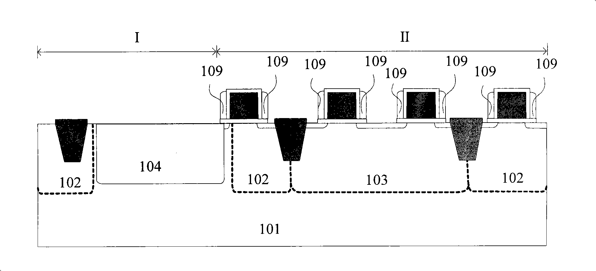
[0025] The invention fully utilizes at least one layer of the first insulating layer forming the polysilicon gate sidewall in the peripheral circuit area to protect the surface of the photodiode, reduces the generation of dark current, and simultaneously does not increase the mask plate. The present invention also removes the first insulating layer remaining on the surface of the photodiode region after forming the side walls of the MOS transistors in the peripheral circuit region, and then forms a second insulating layer in the photodiode region to protect the surface of the photodiode region. Limit the protection scope of the present invention too much. The semiconductor substrate in this embodiment is a p-type silicon substrate, and may also be an n-type silicon substrate, a p- or n-type III-V compound semiconductor substrate, or silicon-on-insulator as the substrate. The protection scope of the present invention should not be limited too much.
[0026]A method for forming...
PUM
 Abstract
Description
Claims
Application Information
 - Generate Ideas
- Intellectual Property
- Life Sciences
- Materials
- Tech Scout
- Unparalleled Data Quality
- Higher Quality Content
- 60% Fewer Hallucinations
Browse by: Latest US Patents, China's latest patents, Technical Efficacy Thesaurus, Application Domain, Technology Topic, Popular Technical Reports.
© 2025 PatSnap. All rights reserved.Legal|Privacy policy|Modern Slavery Act Transparency Statement|Sitemap|About US| Contact US: help@patsnap.com