Method for eliminating residual polymer of etching procedure

A polymer and etching technology, which is applied in the manufacture of electrical components, semiconductor/solid-state devices, circuits, etc., can solve problems such as inability to completely eliminate defects and increase production costs, and achieve the effect of eliminating crown defects, increasing production costs, and being easy to achieve

Inactive Publication Date: 2008-11-19
SEMICON MFG INT (SHANGHAI) CORP
View PDF0 Cites 7 Cited by
  • Summary
  • Abstract
  • Description
  • Claims
  • Application Information

AI Technical Summary

Problems solved by technology

This method can improve the defect situation, but cannot completely eliminate the defect;
[0005] 2. Adding an additional chemical machine polishing (CMP) step, which can eliminate defects, but greatly increases production costs

Method used


Image

  • Method for eliminating residual polymer of etching procedure
  • Method for eliminating residual polymer of etching procedure

Examples


Embodiment Construction

[0012] The process tools used in the semiconductor etching process include a main etch reaction chamber (chamber) for main etching (Main Etch), and a stripping reaction chamber for stripping (strip). Among them, the main etching step removes most of the polysilicon without damaging the gate oxide, and the stripping step removes the previously used resist protection film.

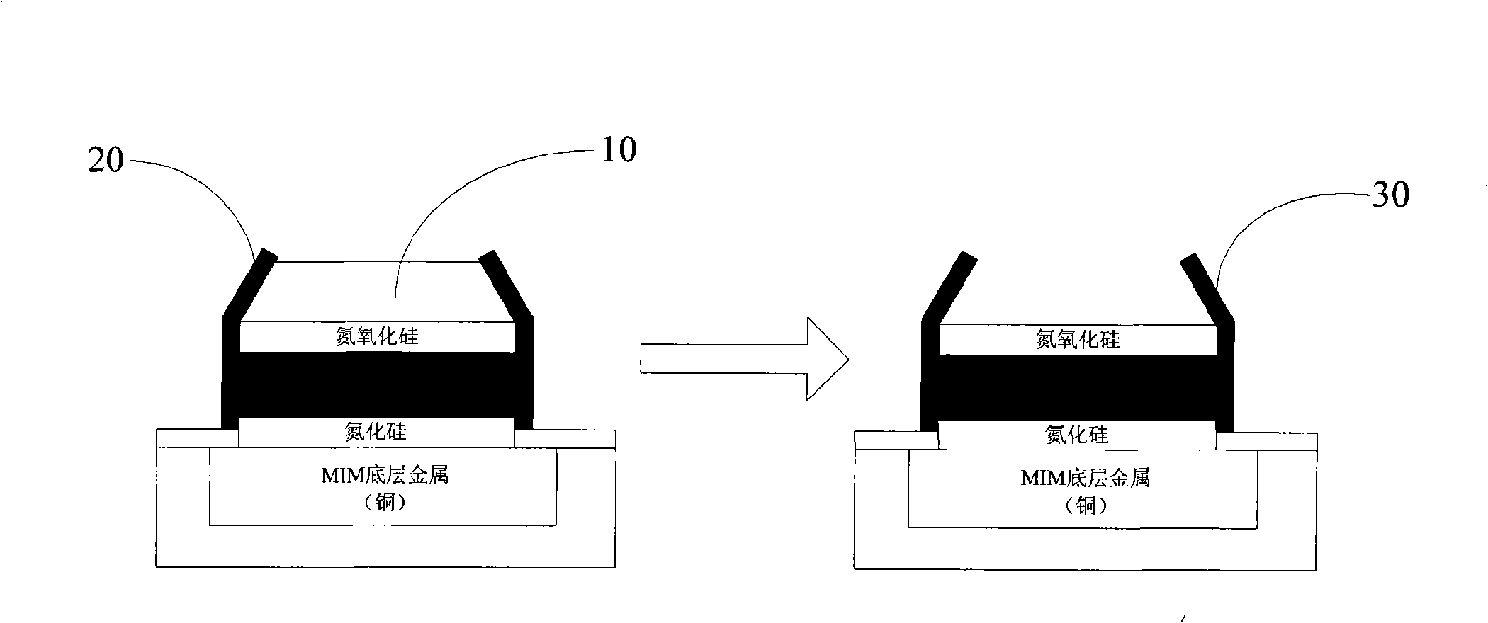
[0013] see figure 1 , is a schematic flow chart of a conventional semiconductor etching process. It proceeds from the main etching step in the main etching reaction chamber to the stripping step in the stripping reaction chamber, at this time, the polymer is produced on the sidewall.

[0014] Generally, etching techniques can be classified into wet etching and dry etching. In wet etching, a chemical solution is used to achieve the purpose of etching through a chemical reaction; dry etching is generally called plasma etching (Plasma Etching). Plasma is a phenomenon in which gas molecules are in a Breakdown...


PUM


Abstract

The invention provides a method to remove residual polymer during etching process. Firstly, a wafer is processed with dry etching in a main etching chamber; then the anticorrosion protective film of the wafer is removed in a decoating chamber; finally, the wafer is again disposed into the main etching chamber for dry etching for the second time; in this way, the residual polymer in the etching process can be gotten rid of. Compared with prior art, the method described by the invention is easy to realize and can thoroughly remove the residual polymer and eliminate coronary defects without increasing production cost by a large margin.

Description

technical field [0001] The invention relates to a semiconductor process method, in particular to a method for eliminating residual polymer in an etching process. Background technique [0002] The etching treatment process is one of the necessary processes in the semiconductor manufacturing process. Its function is to remove the part of the wafer that has not been covered or protected by the photoresist before the development process by chemical reaction or physical action. Among them, the problem of corona defects will be encountered during metal-insulator-metal (Metal-Insulator-Metal, MIM) etching. The generation of this defect is mainly due to the deposition of non-volatile by-products such as tantalum chloride (TaClx) 10 etc. After removal, the crown tantalum chloride polymer 30 is formed. Although there is still a wet cleaning step in the subsequent manufacturing process, this step cannot remove the above-mentioned polymer 30 . [0003] At present, the industry usuall...

Claims


Application Information

Patent Timeline
Patent Type & Authority Applications(China)
IPC IPC(8): H01L21/00H01L21/3065
Inventor 粱昆约许顺富刘凤娇王开立
Owner SEMICON MFG INT (SHANGHAI) CORP
Why Eureka
Try Eureka