

Optical element, method for producing same, replica substrate configured to form optical element, and method for producing replica substrate
A technology of optical components and substrates, which is applied in the field of manufacturing replica substrates, can solve the problems of not being able to fully improve the transmittance characteristics, achieve good anti-reflection characteristics, high transmittance, and improve productivity
- Summary
- Abstract
- Description
- Claims
- Application Information
AI Technical Summary
Problems solved by technology
Method used
Image

Examples
example 1
[0093] Fabrication of Master Molds Configured to Form Optical Elements
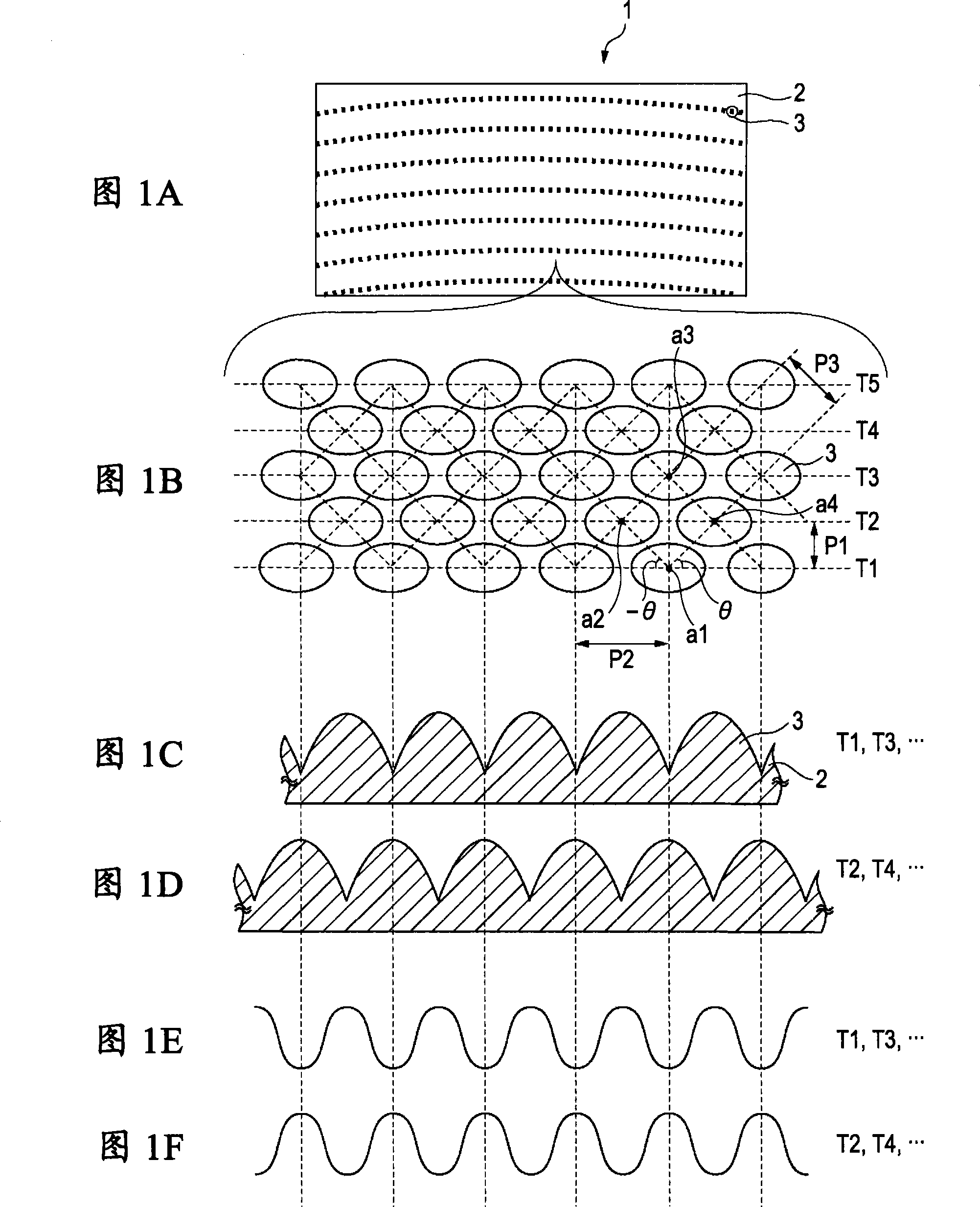
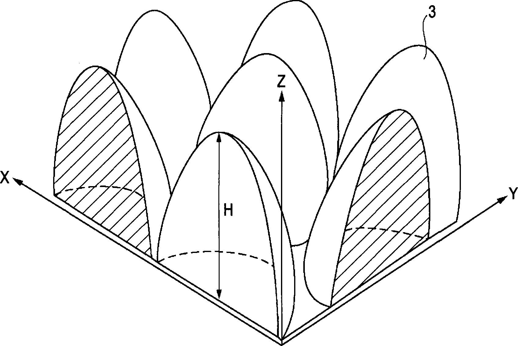
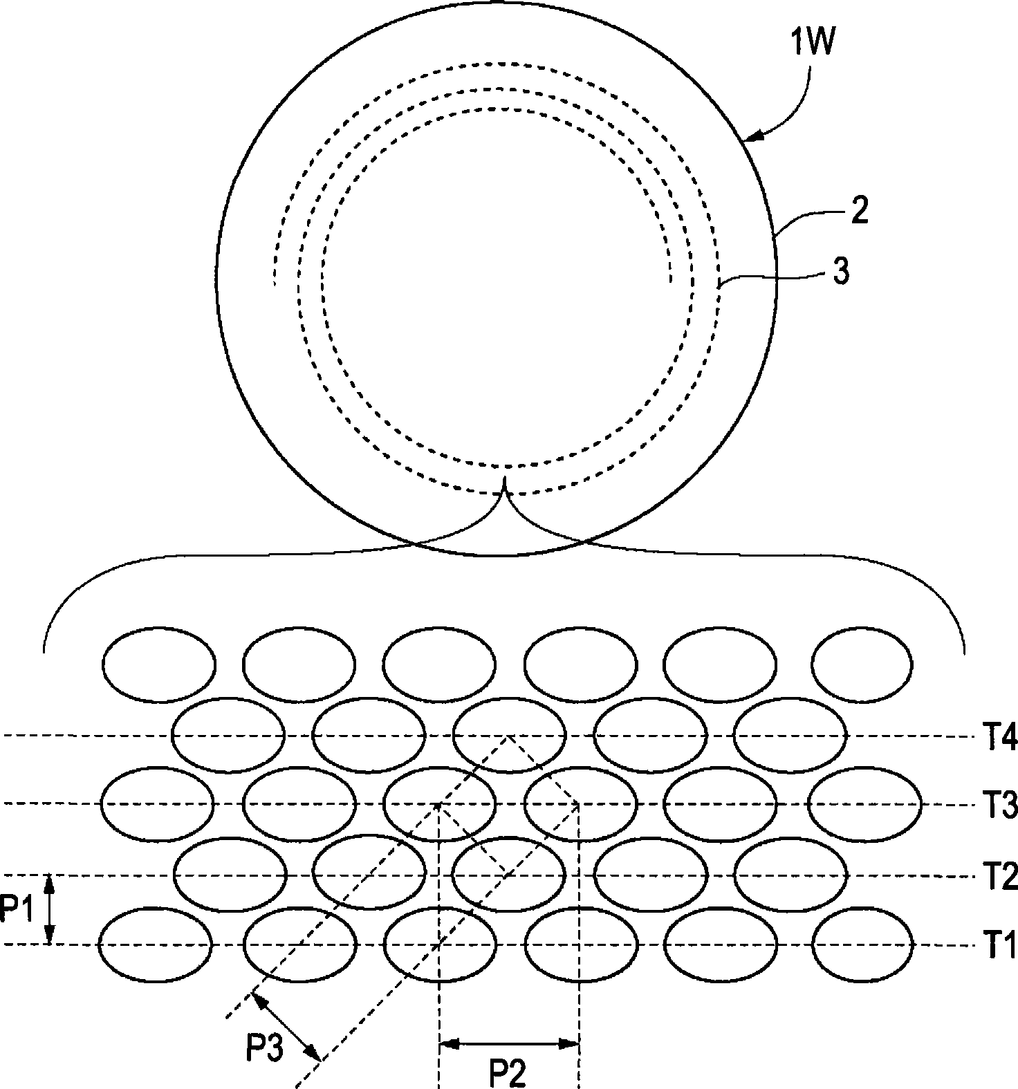
[0094] A chemically amplified or novolac positive resist is applied on the quartz substrate 11 in such a manner that the resist layer 12 has a thickness of about 150 nm. pass Figure 5 The exposure apparatus shown forms latent images 14 arranged in a quasi-tetragonal lattice pattern in the resist layer 12, wherein, in the quasi-tetragonal lattice pattern, the pitch P1 (period in the radial direction) is 190 nm in the radial direction, and the The pitch P2 in the circumferential direction (period in the circumferential direction) was 400 nm, and the pitch P3 in the direction at 45° relative to the circumferential direction (period in the direction at 45° relative to the circumferential direction) was 275 nm. The wavelength of laser light 13 was set to 266 nm. Set the laser power to 0.50 mJ / m. The irradiation period for irradiating the resist layer 12 with the laser light 13 is changed. Then, the resist...
example 2
[0101] are configured to form optical components for fabrication
[0102] In addition to the latent image 14 in a tetragonal lattice pattern (wherein the pitch P1 (period in the radial direction) in the radial direction is 200 nm, the pitch P2 in the circumferential direction (period in the circumferential direction) is 400 nm, and Except that the pitch P3 in the direction of 45° (the period in the direction of 45° relative to the circumferential direction) is 283 nm), a resist pattern in the form of a tetragonal lattice was formed as in Example 1.
[0103] Next, polishing and etching are performed as follows: (1) Oxygen polishing for five seconds and CHF 3 Etch for one minute; (2) perform oxygen polishing for five seconds and perform CHF 3 Etch for two minutes; (3) perform oxygen polishing for five seconds and perform CHF 3 Etch for three minutes; and (4) Oxygen polish for five seconds with CHF 3 Etch for four minutes. Then, oxidation polishing was performed for 10 second...
example 3
[0108] Fabrication of Master Molds Configured to Form Optical Elements
[0109] In addition to the latent image 14 in a tetragonal lattice pattern (wherein, the pitch P1 (period in the radial direction) in the radial direction is 210 nm, the pitch P2 (period in the circumferential direction) in the circumferential direction is 420 nm, and The pitch P3 in the direction of 45° (period in the direction of 45° with respect to the circumferential direction) is 297 nm) arrangement, as in Example 1, a resist pattern in the form of a tetragonal lattice was formed.
[0110] Next, polishing and etching are performed as follows: (1) Oxygen polishing for five seconds and CHF 3 Etch for one minute; (2) perform oxygen polishing for five seconds and perform CHF 3 Etch for two minutes; (3) perform oxygen polishing for five seconds and perform CHF 3 Etch for three minutes; and (4) Oxygen polish for five seconds with CHF 3 Etch for four minutes. Then, oxidation polishing was performed for 1...
PUM
| Property | Measurement | Unit |
|---|---|---|
| depth | aaaaa | aaaaa |
| thickness | aaaaa | aaaaa |
| thickness | aaaaa | aaaaa |
Abstract
Description
Claims
Application Information