High on-stage voltage right-handed LED integrated chip and manufacturing method thereof

An integrated chip, high-conduction technology, applied in semiconductor/solid-state device manufacturing, circuits, electrical components, etc., can solve the problem of poor high-voltage resistance of LED integrated chips, and achieve small footprint, good thermal conductivity, and low cost Effect

Inactive Publication Date: 2008-12-24
NANKER GUANGZHOU SEMICON MFG
View PDF0 Cites 4 Cited by
  • Summary
  • Abstract
  • Description
  • Claims
  • Application Information

AI Technical Summary

Problems solved by technology

Therefore, the high-voltage resistance performance of the existing LED integrated chip is not good

Method used


Image

  • High on-stage voltage right-handed LED integrated chip and manufacturing method thereof
  • High on-stage voltage right-handed LED integrated chip and manufacturing method thereof
  • High on-stage voltage right-handed LED integrated chip and manufacturing method thereof

Examples


Embodiment 1

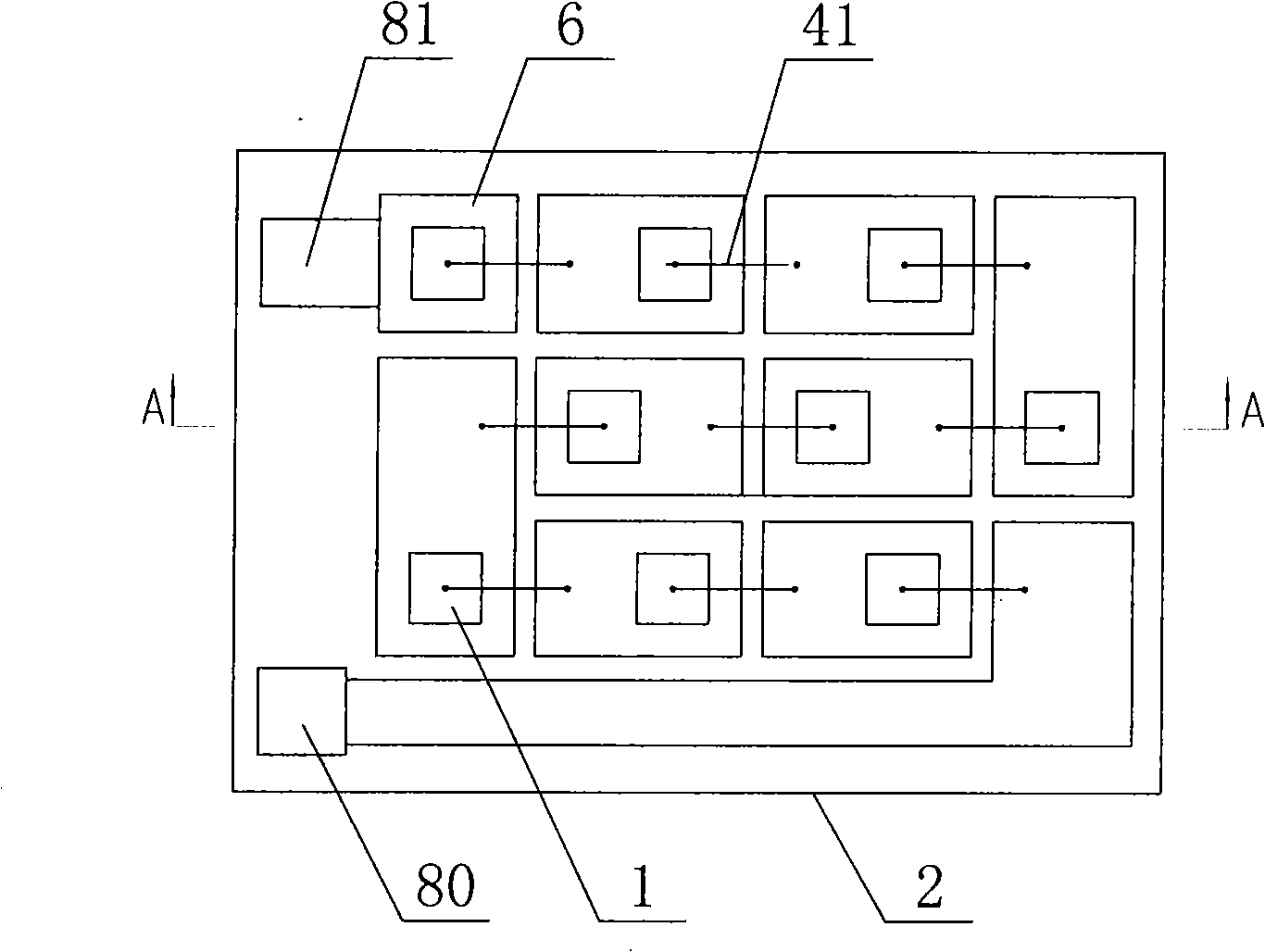
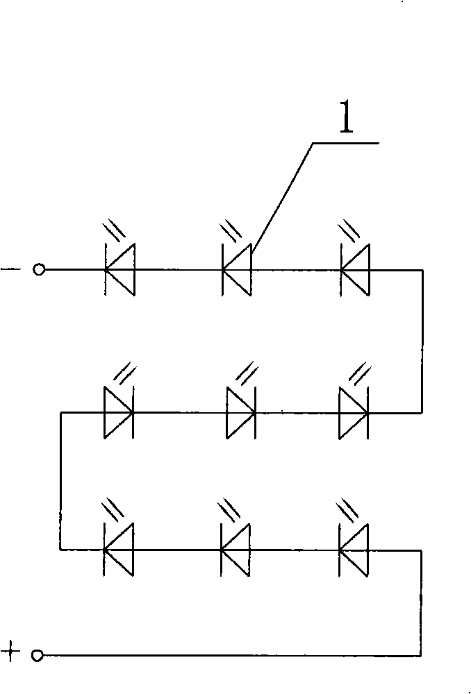
[0045] Such as figure 1 , image 3 , Figure 4 As shown, the high conduction voltage front-mounted LED integrated chip of this embodiment includes nine LED bare chips 1 and a silicon substrate 2, the LED bare chips 1 are single-electrode chips, and the LED bare chips 1 include gallium arsenide ( GaAs) substrate 10 and N-type epitaxial layer 11, P-type epitaxial layer 12, certainly, described substrate 10 also can be the substrate of other materials such as silicon carbide (SiC), described silicon substrate 2 is P-type silicon substrate, the front side of the silicon substrate 2 is formed with a thermally conductive insulating layer, and the thermally conductive insulating layer is solely composed of a second thermally conductive insulating layer 5 formed by deposition, and the second thermally conductive insulating layer 5 is composed of a silicon nitride layer, The thermal conductivity of silicon nitride is very high, and its thermal conductivity is more than 100 times high...

Embodiment 2

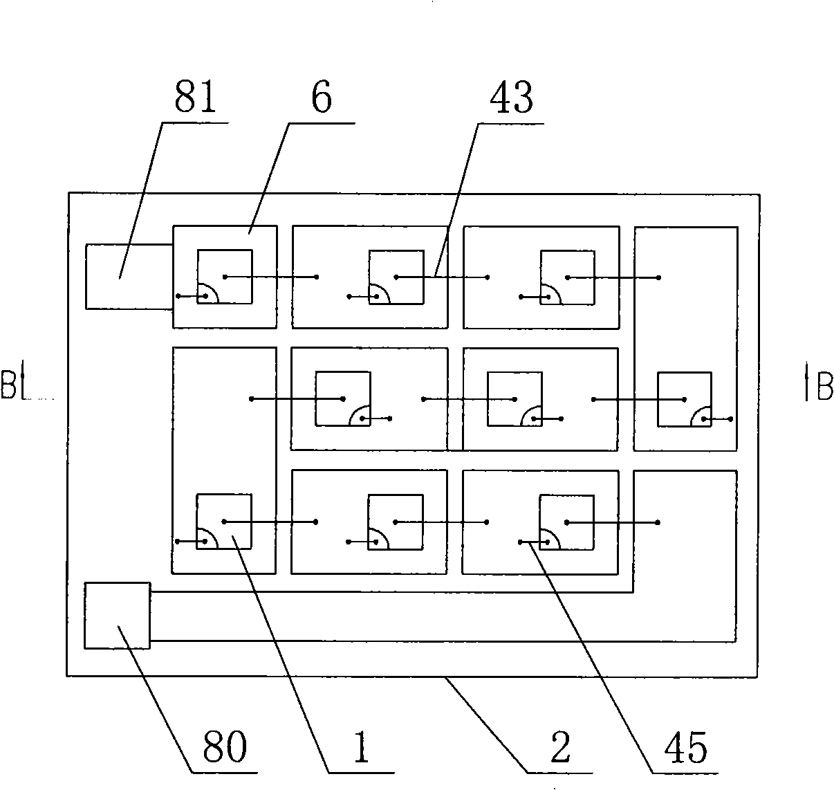
[0054] Such as figure 2 , image 3 , Figure 5 to Figure 9 As shown, the difference between this embodiment and Embodiment 1 is that: the LED bare chip 1 is a double-electrode chip, and the substrate 10 is aluminum oxide (sapphire, Al 2 o 3 ) substrate, the P-type epitaxial layer 12 and the N-type epitaxial layer 11 are soldered to two adjacent metal layers 6 through metal wires 43 and 45 respectively.

[0055] The remaining features of this embodiment are the same as those of Embodiment 1.

Embodiment 3

[0057] Such as figure 1 , image 3 , Figure 10 As shown, the difference between the high turn-on voltage front-mounted LED integrated chip of this embodiment and the first embodiment is that a layer of N+ diffusion layer 3 is diffused inwardly from the front side of the silicon substrate 2 described in this embodiment, and the N+ A first thermally conductive insulating layer 4 is grown on the diffusion layer 3, a second thermally conductive insulating layer 5 is deposited on the first thermally conductive insulating layer 4, and a metal layer 6 is deposited on the second thermally conductive insulating layer 5, that is, the The thermally conductive insulating layer is composed of the first thermally conductive insulating layer 4 formed by growth and the second thermally conductive insulating layer 5 formed by deposition, the first thermally conductive insulating layer 4 is made of silicon dioxide, and the second thermally conductive insulating layer 5 is composed of silicon...


PUM


Abstract

The invention discloses a high continuity voltage up-mounted LED integrated chip with static protection which has the advantages of low cost, easy integration, good heat dissipation effect and high-pressure resistance and a manufacturing method thereof. The integrated chip comprises a plurality of LED bare chips (1) and silicon substrates (2), wherein, the LED bare chips (1) comprise substrates (10), N-type epitaxial layers (11) and P-type epitaxial layers (12), heat conducting insulating layers are formed on the front surfaces of the silicon substrates (2), metal layers (6) are deposited on the heat conducting insulating layers, the LED bare chips (1) are up-mounted on the metal layers (6) and are connected through the metal layers (6) to form a circuit, anode contacts (80) and cathode contacts (81) are led out from the metal layers (6). The manufacturing method comprises the following steps: forming the heat conducting insulating layers, forming the metal layer and encapsulating the LED bare chips, and is widely applicable to the LED bare chip field.

Description

technical field [0001] The invention relates to a high conduction voltage front-mounted LED integrated chip; in addition, the invention also relates to a manufacturing method of the high conduction voltage front-mounted LED integrated chip. Background technique [0002] Front-mount chip technology is a traditional microelectronic packaging technology, which is mature and widely used. At present, the vast majority of LEDs are formal-mounted LEDs. Whether the substrate of the LED bare chip is gallium arsenide or silicon carbide, a layer of metal is plated on the outside of the substrate as an N-type electrode, and it is also used for heat dissipation. A bracket with a reflective cup is used as the cathode, and the P-type epitaxial layer on it is welded to the anode lead through a metal wire. Since the top of the bare chip and the substrate surface are used as one end of the electrode, it is commonly called "single Electrode chip", at present, yellow light and red light LED mo...

Claims


Application Information

Patent Timeline
Patent Type & Authority Applications(China)
IPC IPC(8): H01L25/075H01L23/36H01L23/488H01L21/48H01L21/50H01L21/60
CPCH01L2224/48091H01L2224/49107H01L2224/73265H01L2924/1301
Inventor 吴俊纬
Owner NANKER GUANGZHOU SEMICON MFG
Why Eureka
Try Eureka