Encapsulation construction of LED

A light-emitting diode and packaging structure technology, which is applied in the direction of electrical components, circuits, semiconductor devices, etc., can solve the problems of inability to meet the miniaturized light-emitting diode packaging structure, poor heat resistance, unfavorable light reflection, etc., and achieve excellent reflection and durability. Effects of thermal characteristics, prolonging service life, and improving light extraction efficiency

Active Publication Date: 2009-01-07
AU OPTRONICS CORP
View PDF0 Cites 7 Cited by
  • Summary
  • Abstract
  • Description
  • Claims
  • Application Information

AI Technical Summary

Problems solved by technology

[0003] However, it is well known that in terms of the existing light emitting diode packaging structure, taking the reflection cup structure as an example, it can be made of resin or ceramic materials, wherein the heat conduction effect of the reflection cup of ceramic material is better than that of resin material, but , the light-emitting diode package structure made of ceramic materials (such as: aluminum nitride) can only reach the specifications of about 3.0 mm * 2.0 mm * 1.2 mm in the minimum size limit of length, width, and height, and can only be formed with a right-angle shape. The packaging structure of the state cannot meet the needs of the miniaturized LED packaging structure, and is not conducive to the reflection of light. Therefore, for portable display devices that need to use the miniaturized LED packaging structure as a light source, it is still necessary to use a resin material ( Example: Reflective cup made of poly(p-phenylene terephthalamide, PPA)
However, due to the poor heat resistance of the resin material itself, for example, after 126 hours of operation at an operating temperature of 140 degrees Celsius, poly-p-phenylene terephthalamide will have obvious yellowing and deterioration problems

Method used


Image

  • Encapsulation construction of LED
  • Encapsulation construction of LED
  • Encapsulation construction of LED

Examples


Embodiment Construction

[0033] A light emitting diode packaging structure according to a preferred embodiment of the present invention will be described below with reference to related drawings.

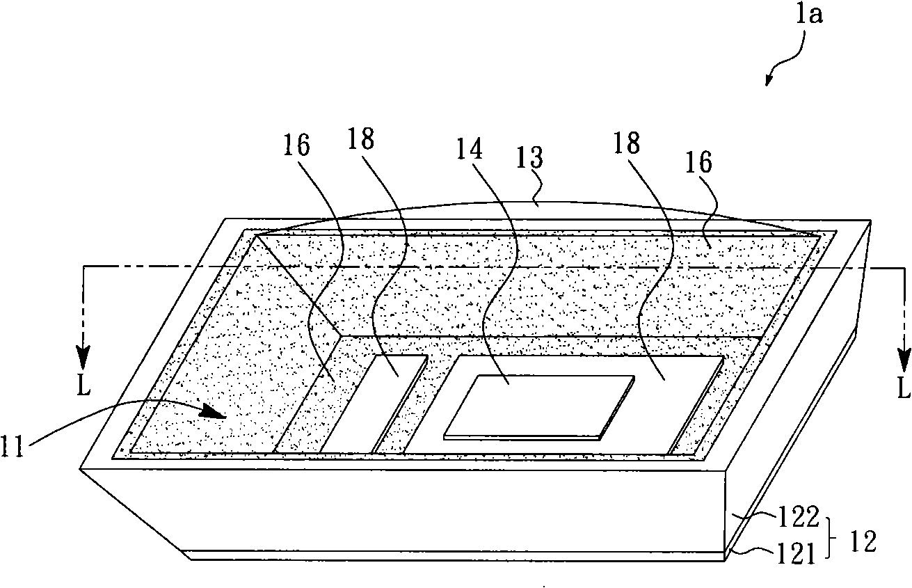
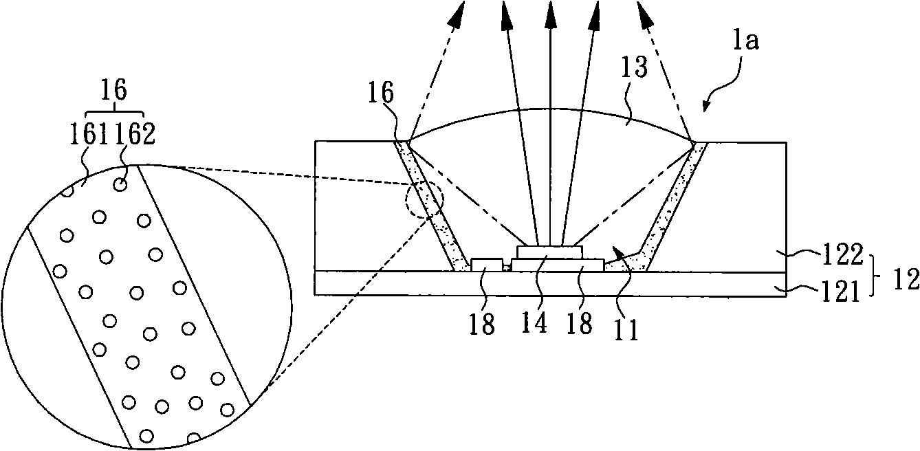
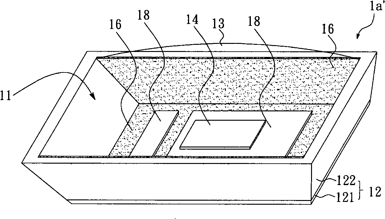
[0034] First, please also refer to Figure 1A , Figure 1B and Figure 1C shown, where Figure 1A is a perspective view of the LED packaging structure, and Figure 1B then along Figure 1A A cross-sectional view of the light-emitting diode package structure at the mid-section line L, Figure 1C then Figure 1A Another perspective view of .

[0035] First, according to Figure 1A and Figure 1B It can be seen that the LED package structure 1 a shown in the figure includes a carrying unit 12 , a LED chip 14 , a composite material layer 16 and a reflective electrode 18 . A reflective electrode 18 is set between the carrying unit 12 and the LED chip 14, in other words, the reflective electrode 18 is set on the carrying unit 12, and the light emitting diode chip 14 is located on the reflective electrode 18...


PUM

PropertyMeasurementUnit
wavelengthaaaaaaaaaa
thicknessaaaaaaaaaa
reflectanceaaaaaaaaaa

Abstract

The invention provides an LED package structure which comprises a bearing unit, an LED chip and a composite material layer. The LED chip is positioned on the bearing unit; and the composite material layer is partially or completely covered on the surface of the bearing unit which is close to the LED chip; wherein, the composite material layer comprises resin material and inorganic dielectric material, and the resin material is provided with a first refraction coefficient; the inorganic dielectric material is mixed in the resin material and is provided with a second refraction coefficient, wherein, the first refraction coefficient is less than the second refraction coefficient, and the difference value between the first refraction coefficient and the second refraction coefficient is at least more than 0.2. The LED package structure can increase ray reflectivity of the LED package structure by modifying materials, which improves the light emitting efficiency of the LED package structure and greatly prolongs the service life of the LED package structure.

Description

technical field [0001] The invention relates to a light emitting diode packaging structure, in particular to a light emitting diode packaging structure with high reflectivity and high heat resistance. Background technique [0002] In response to the goal of saving energy, it has become the mainstream research of luminous technology to find out the luminous source that can replace the known poor luminous efficiency. In terms of the current technology, the most potential alternative luminous source should be the light-emitting diode. [0003] However, it is well known that in terms of the existing light emitting diode packaging structure, taking the reflection cup structure as an example, it can be made of resin or ceramic materials, wherein the heat conduction effect of the reflection cup of ceramic material is better than that of resin material, but , the light-emitting diode package structure made of ceramic materials (such as: aluminum nitride) can only reach the specifica...

Claims


Application Information

Patent Timeline
Patent Type & Authority Applications(China)
IPC IPC(8): H01L33/00H01L33/48H01L33/54
Inventor 杨健理洪春长林睿腾
Owner AU OPTRONICS CORP
Why Eureka
Try Eureka