Method for forming graphic pattern

A patterning and patterning technology, applied in electrical components, semiconductor/solid-state device manufacturing, circuits, etc., can solve the problems of inability to achieve line width, increase process costs, etc., and achieve the effect of increasing integration.

Active Publication Date: 2009-01-14
MACRONIX INT CO LTD
View PDF0 Cites 9 Cited by
  • Summary
  • Abstract
  • Description
  • Claims
  • Application Information

AI Technical Summary

Problems solved by technology

However, even in combination with other resolution-enhancing technologies, for the 248nm lithography process, it is still impossible to form a line width below 100nm
Furthermore, improving the equipment and materials used in the current lithography system to meet the needs of the lithography process will also increase the cost of the process

Method used


Image

  • Method for forming graphic pattern
  • Method for forming graphic pattern
  • Method for forming graphic pattern

Examples


Embodiment Construction

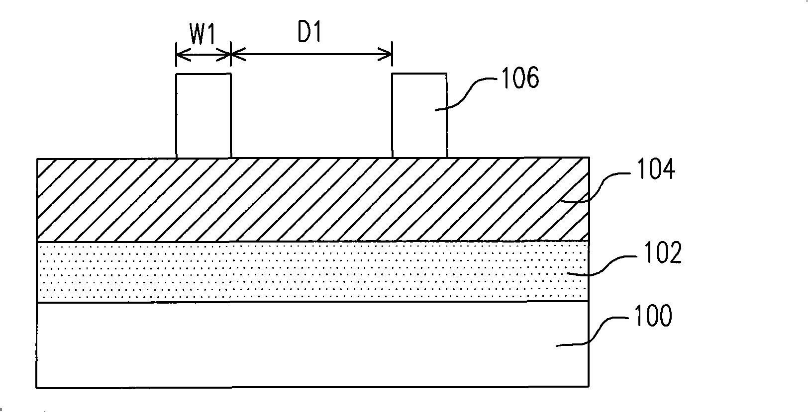
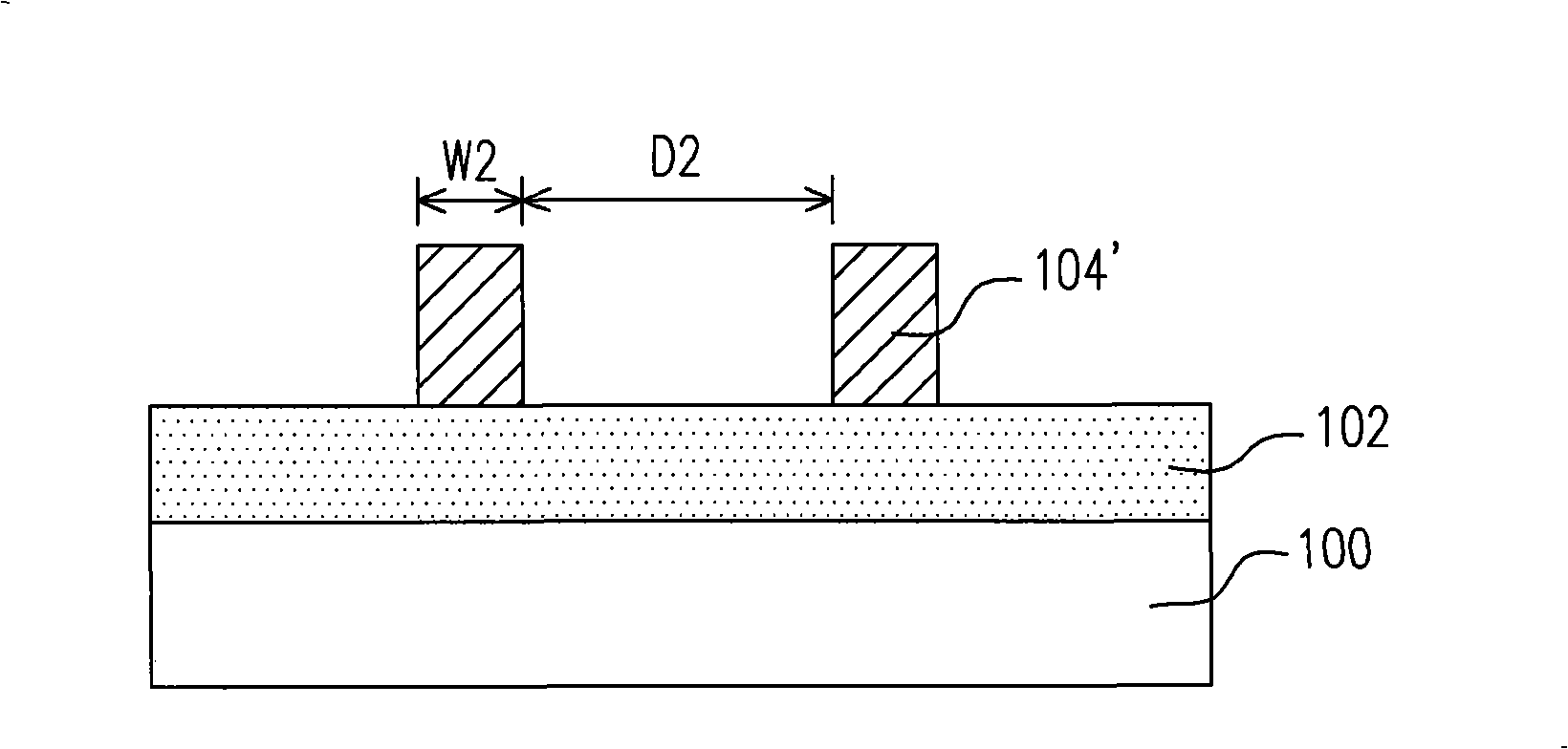
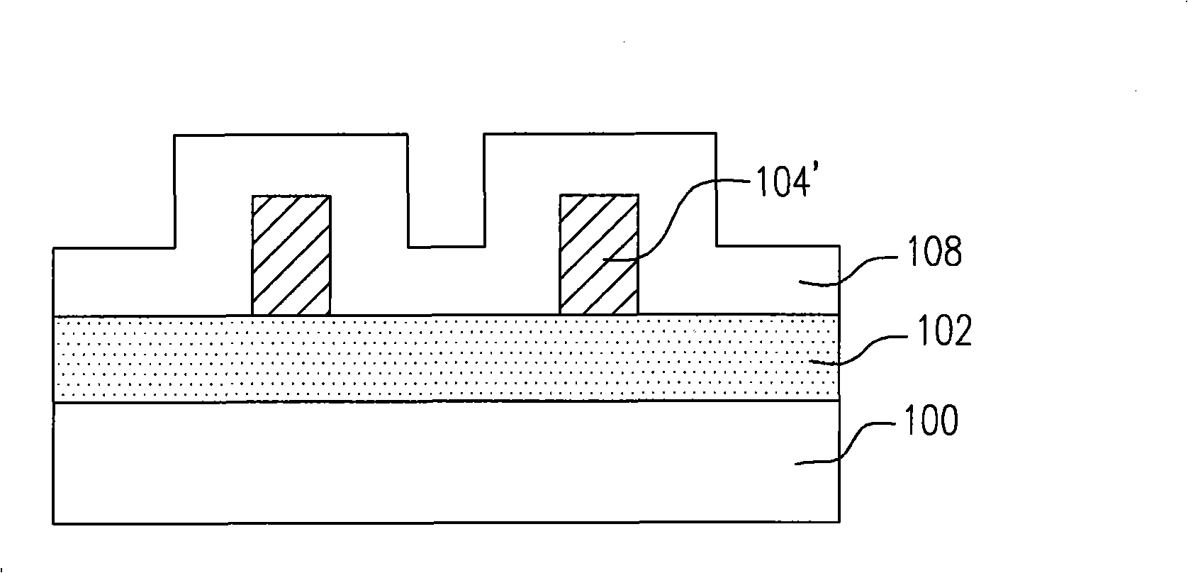
[0025] 1A to 1G It is a cross-sectional view of a manufacturing process of a pattern according to an embodiment of the present invention.

[0026] First, please refer to Figure 1A , a material layer 100 is provided. The material layer 100 is, for example, a polysilicon layer, a dielectric layer or a metal layer. The formation method of the material layer 100 is, for example, a physical vapor deposition process or a chemical vapor deposition process, which can be adjusted according to different material requirements. After that, a mask layer 102 is formed on the material layer 100 . The material of the mask layer 102 is, for example, nitride or oxide. The formation method of the mask layer 102 is, for example, a chemical vapor deposition process. Subsequently, a hard mask layer 104 is formed on the mask layer 102 . The material of the hard mask layer 104 is, for example, nitride or oxide. The formation method of the hard mask layer 104 is, for example, a chemical vapor ...


PUM


Abstract

The invention provides a forming method of a pattern, comprising the steps as follows: firstly, a material layer is provided; a patterned hard mask layer is formed on the material layer; subsequently, a clearance wall is respectively formed on the side wall of the patterned hard mask layer; subsequently, the patterned hard mask layer is removed and an opening is formed between the two adjacent clearance walls; subsequently, the clearance wall is used as the mask so as to remove a part of material layer, thus forming a patterned material layer.

Description

technical field [0001] The present invention relates to a method for forming a pattern, and more particularly, to a method for forming a pattern having the same line width and line spacing. Background technique [0002] As the integration level of integrated circuits becomes higher and higher, the design of the size of the entire semiconductor element is also forced to move forward in the direction of continuous reduction in size. In other words, if the packing density of components and the integration degree of integrated circuits are to be increased, the pattern pitch, that is, the sum of the line width and the line pitch of the pattern, must also be reduced accordingly. Generally speaking, in the manufacturing process of integrated circuits, the pattern pitch is mostly reduced by a high-resolution lithography process, that is to say, the line width and line spacing are determined by the photoresist layer after exposure and development. [0003] One of the ways to increas...

Claims


Application Information

Patent Timeline
Patent Type & Authority Applications(China)
IPC IPC(8): H01L21/027H01L21/033H01L21/308H01L21/311H01L21/3213
Inventor 蔡世昌李俊鸿郑明正杨大弘
Owner MACRONIX INT CO LTD
Why Eureka
Try Eureka