Method for forming micro-graphic pattern on floating grid

A micro-pattern, floating gate technology, applied in electrical components, semiconductor/solid-state device manufacturing, circuits, etc., can solve problems such as high cost, inability to meet the requirements of critical dimensions for detection, and small process tolerance, achieving easy implementation, good The effect of pattern reproducibility and process cycle saving

Inactive Publication Date: 2009-01-14
SEMICON MFG INT (SHANGHAI) CORP +1
View PDF0 Cites 1 Cited by
  • Summary
  • Abstract
  • Description
  • Claims
  • Application Information

AI Technical Summary

Problems solved by technology

[0004] However, due to the limitation of the resolution of the 248nm KrF scanner, the current photolithography technology for forming lines and spaces on floating gates cannot achieve line spacing of 80nm or below through the traditional 248nm KrF process, so it cannot meet the required development. Requirements for post-inspection critical dimensions
[0005] Although 193nm ArF can be done, its cost is relatively high and its process tolerance is small

Method used


Image

  • Method for forming micro-graphic pattern on floating grid
  • Method for forming micro-graphic pattern on floating grid
  • Method for forming micro-graphic pattern on floating grid

Examples


Embodiment

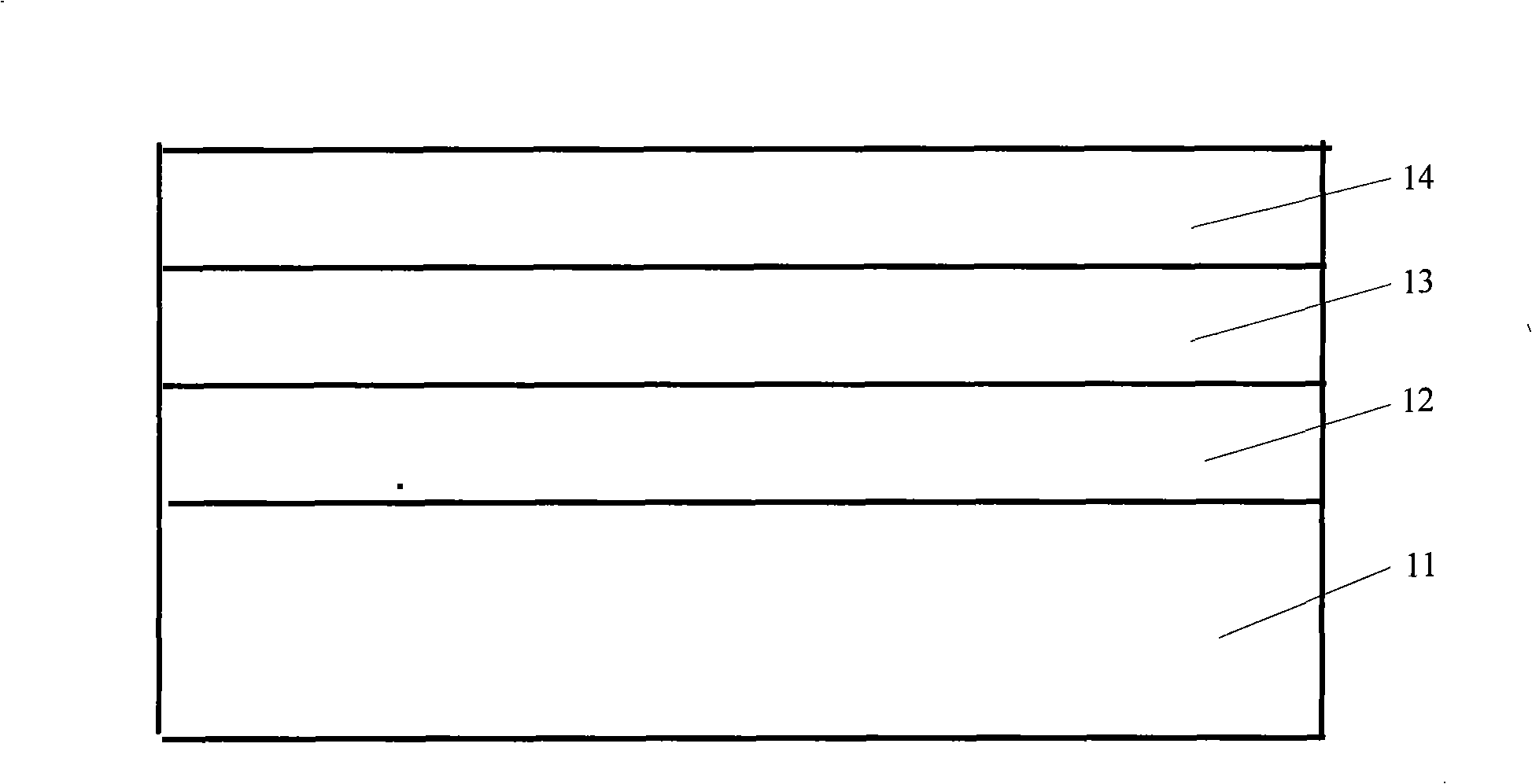
[0039] Take the case of forming a floating gate structure of NAND flash memory with 0.22 μm line and 80 nm interval as an example.

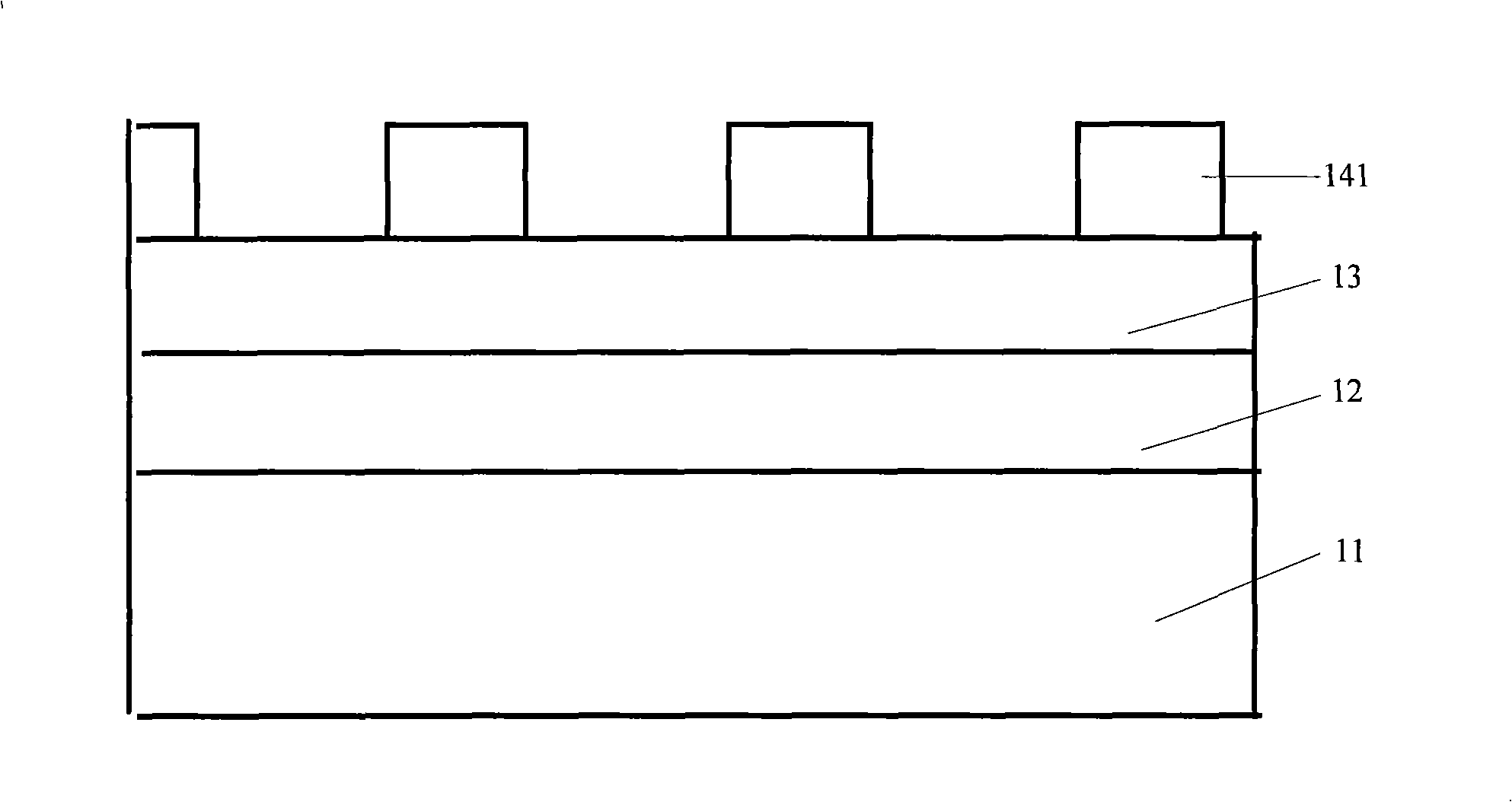
[0040] A polysilicon layer 22 is sequentially formed on a silicon substrate 21 with a thickness of 7500 The photoresist layer 23, such as Figure 2A shown;

[0041] Use a KrF (ASML PAS / 850C) scanner to expose and develop the photoresist layer 23 to form a pattern 231 with a line width of 0.14 μm and a space of 0.16 μm, as Figure 2B shown;

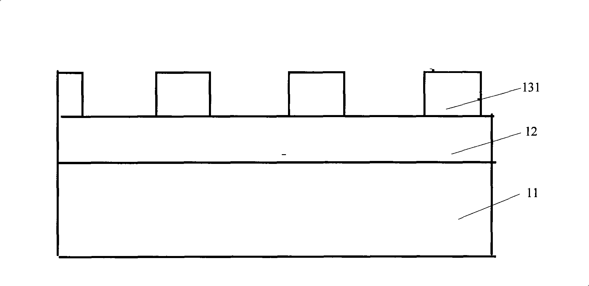
[0042] The formed photoresist pattern is generally baked at a temperature between 80° C. and the glass transition temperature (Tg) of the photoresist for 80 to 200 seconds, and the baking is performed on a heating plate.

[0043] After the above process, due to the addition of a baking step after development, that is, a thermal reflow step, this step causes the photoresist to reflow, thereby making the line width of the pattern larger and rounder, and as a result, the developed size of the space will be r...


PUM


Abstract

The invention provides a method for forming micro-fine patterns on a floating grid, comprising the steps as follows: a multi-crystal silicon layer and a photoresist layer are sequentially formed on a silicon substrate where a floating grid is formed; the photoresist layer is exposed and developed; thermal reflux is carried out to the obtained photoresist patterns; by controlling the reflux temperature and the reflux time, the photoresist patterns with prearranged wire width and spacing are obtained; subsequently, the photoresist patterns with the prearranged wire width and the spacing is transferred to the multi-crystal silicon layer so as to carry out the subsequent preparation. By the method of the invention, patterns with the spacing of 80nm and less than 80nm on the floating grid, which can only be obtained by the more advanced ArF(ASML PAS/1150C) scanner and ArF photoresist, can be obtained only by adopting the KrF(ASML PAS/850c) scanner and thermal reflux KrF photoresist; furthermore, by comparison, the preparation process tolerance is more.

Description

technical field [0001] The invention relates to a method related to the manufacture of a non-flash memory, especially a method for manufacturing a fine pattern on a floating gate. Background technique [0002] For NAND flash memory, it is necessary to make a pattern with 80nm spacing / 0.22μm line width on the floating gate. [0003] The traditional method is to sequentially form a polysilicon layer, a silicon nitride layer, and a photoresist layer on the substrate; To complete the formation of the photoresist pattern; then etch the silicon nitride layer, and then etch the polysilicon layer using the silicon nitride as a mask to form a line interval much larger than 80nm. The line spacing is then narrowed to 80nm by forming polysilicon spacers. [0004] However, due to the limitation of the resolution of the 248nm KrF scanner, the current photolithography technology for forming lines and spaces on floating gates cannot achieve line spacing of 80nm or below through the tradit...

Claims


Application Information

Patent Timeline
Patent Type & Authority Applications(China)
IPC IPC(8): H01L21/8247H01L21/768H01L21/308
Inventor 崔彰日邱何
Owner SEMICON MFG INT (SHANGHAI) CORP
Why Eureka
Try Eureka