Method for preparing microwave high-frequency multi-layer circuit board

A multi-layer circuit board and manufacturing method technology, applied in the direction of multi-layer circuit manufacturing, etc., can solve the problems of reducing the stability of the circuit board, large dielectric loss, large dielectric constant, etc., to meet mass production, improve bonding force, The effect of improving the bonding force between layers

Active Publication Date: 2009-01-21
TAIZHOU BOTAI ELECTRONICS
View PDF0 Cites 19 Cited by
  • Summary
  • Abstract
  • Description
  • Claims
  • Application Information

AI Technical Summary

Problems solved by technology

[0002] With the development of electronic products in the direction of miniaturization, high frequency, digitalization, and high reliability, epoxy resin board (FR-4) is used as the adhesive sheet in the process of microwave high frequency multilayer circuit board at present, but It has a single variety, low solderability, large dielectric loss, and a large dielectric constant. In addition, the hole wall is treated with sodium salt solution in the current production process, but this reduces the stability of the circuit board, especially is storage stability

Method used


Image

  • Method for preparing microwave high-frequency multi-layer circuit board

Examples


Embodiment Construction

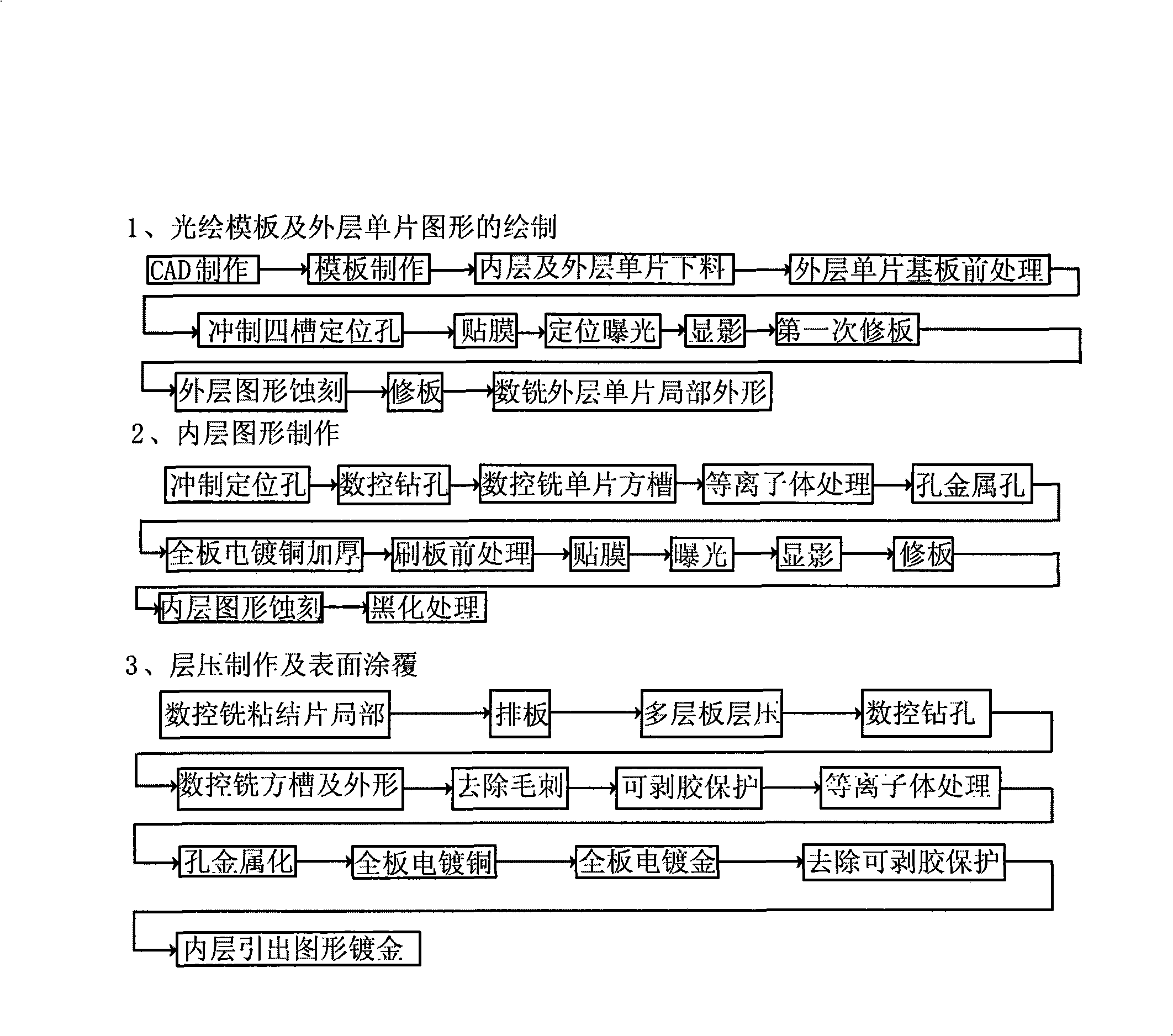
[0009] exist figure 1 Among them, the present invention provides a kind of manufacture method of microwave high-frequency multilayer circuit board, and it comprises the following steps: Step 1, the making of optical drawing template and outer layer figure: 1, adopt CAD in the inner and outer layer monolithic of template Graphic design on the board, the inner monolithic board and the outer monolithic board are made of glass fiber reinforced tetrafluoroethylene copper clad board, ceramic filled PTFE copper clad board or ceramic filled thermosetting resin copper clad board , 2. Blanking the inner and outer monolithic boards of the template, 3. Punching four slot positioning holes on the outer monolithic board, 4. Sticking a film on the outer monolithic board, performing positioning exposure and developing, according to the image Such as repairing the outer monolithic board, 5. Etching according to the designed graphics on the outer monolithic board, and then performing the second...


PUM


Abstract

The invention discloses a making method of a microwave and high frequency multilayer circuit board, and the method comprises the following steps: step one, making gerber templates and outer graphics; step two, making inner graphics; step three, laminated making and surface coating. The making method is high in precision and steady in the performance of the made circuit board, and besides dielectric constants are stable and dielectric loss is small.

Description

technical field [0001] The invention relates to a method for manufacturing a microwave high-frequency multilayer circuit board, in particular to a method for manufacturing a multilayer circuit board used in high-frequency signal transmission electronic products and high-speed logic signal transmission electronic products. Background technique [0002] With the development of electronic products in the direction of miniaturization, high frequency, digitalization, and high reliability, epoxy resin board (FR-4) is used as the adhesive sheet in the process of microwave high frequency multilayer circuit board at present, but It has a single variety, low solderability, large dielectric loss, and a large dielectric constant. In addition, the hole wall is treated with sodium salt solution in the current production process, but this reduces the stability of the circuit board, especially is storage stability. Contents of the invention [0003] The invention provides a method for ma...

Claims


Application Information

Patent Timeline
Patent Type & Authority Applications(China)
IPC IPC(8): H05K3/46
Inventor 施吉连
Owner TAIZHOU BOTAI ELECTRONICS
Why Eureka
Try Eureka