Check patentability & draft patents in minutes with Patsnap Eureka AI!

Disposable programmable memory circuit and programming and reading method thereof

A memory circuit, a one-time technology, applied in the semiconductor field, can solve problems such as the influence of the data reading process of the programmable memory, and achieve the effects of improving the programming speed, improving the reliability and reducing the cost.

Active Publication Date: 2009-02-04
GIGADEVICE SEMICON (BEIJING) INC
View PDF0 Cites 4 Cited by
  • Summary
  • Abstract
  • Description
  • Claims
  • Application Information

AI Technical Summary

Problems solved by technology

[0003] Since the data programming and reading operations of the existing programmable memory share a bidirectional data input and output channel, it is easy to cause the influence of the data reading process of the programmable memory during the data programming operation of the programmable memory

Method used


Image

  • Disposable programmable memory circuit and programming and reading method thereof
  • Disposable programmable memory circuit and programming and reading method thereof
  • Disposable programmable memory circuit and programming and reading method thereof

Examples


Embodiment Construction

[0048] Specific embodiments of the present invention will be described in detail below in conjunction with the accompanying drawings.

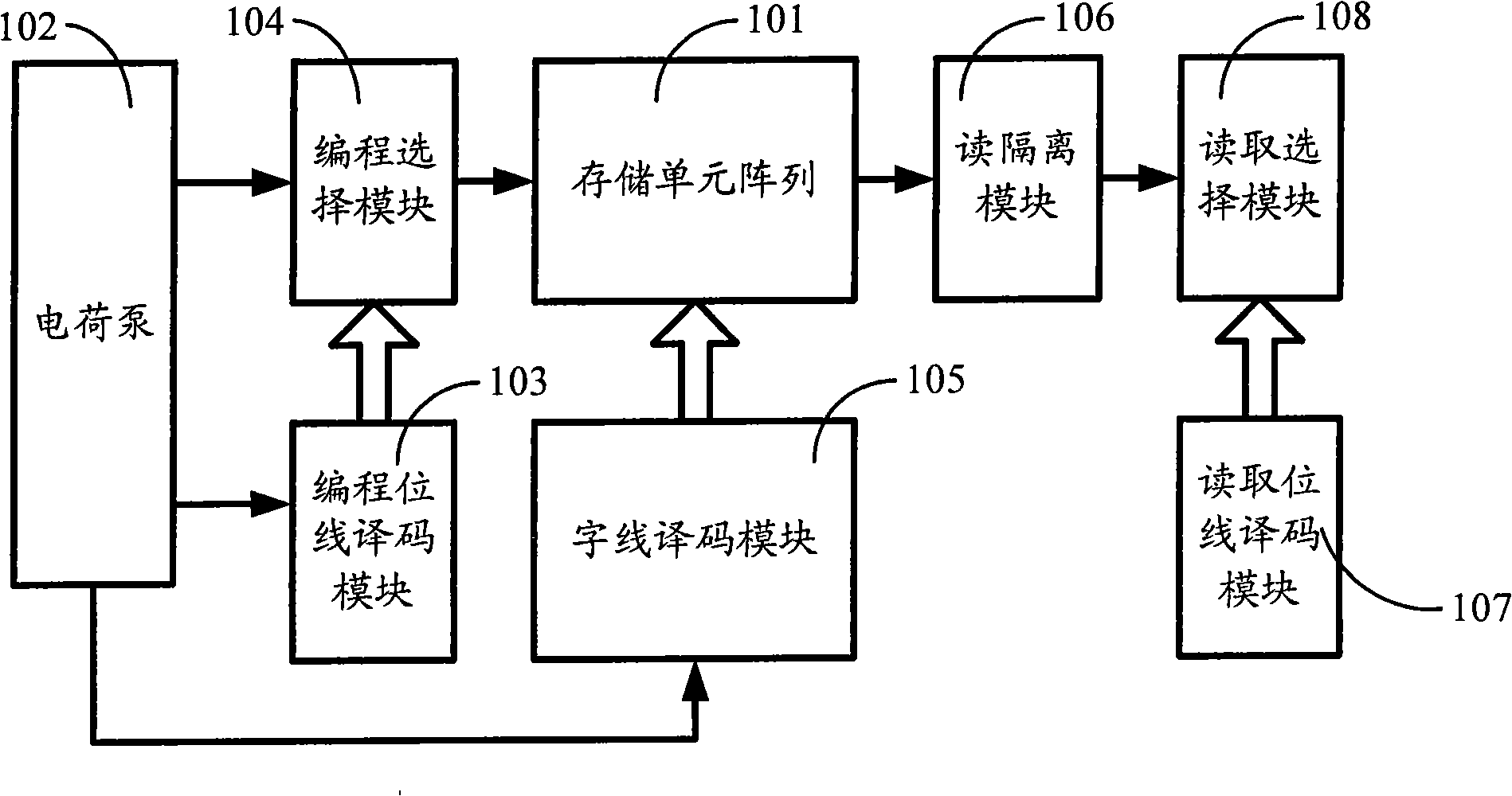
[0049] figure 1 It is a structural block diagram of a one-time programmable memory circuit in a specific embodiment of the present invention, which includes a memory cell array 101, a charge pump 102, a programming bit line decoding module 103, a programming selection module 104, a word line decoding module 105, a read An isolation module 106 , a read bit line decoding module 107 and a read selection module 108 . in,

[0050] The memory cell array 101 is used for storing data. The memory cell array 101 includes a plurality of memory cells, wherein each memory cell includes such as Figure 4a The P-type MOS transistor P41 as a selection transistor and the P-type MOS transistor P42 as a data storage transistor are shown, wherein the gate oxide layer of the MOS transistor P42 is thinner than that of an ordinary MOS transistor; or as Figure 4...


PUM


Abstract

The invention discloses an OTP (one time programmable) memory circuit and a programming and read method. The OTP memory circuit comprises a memory cell array, a charge pump, a word line encoding module, a programming bit line encoding module, a programming selecting module, a read isolating module, a read bit line encoding module and a read selecting module. Through the read isolating module, the OTP memory circuit prevents the high voltage on the programming bit line from puncturing the transistors connected to the read bit line during data programming, thus effectively avoiding influence to the data read operation from the high voltage generated during the data programming operation and improving the reliability of the programming and read of the OTP memory.

Description

technical field [0001] The present invention mainly relates to semiconductor technology, in particular to a one-time programmable memory circuit and its programming and reading methods. Background technique [0002] During the design process of a system on chip (SOC, System On Chip) based on a logic process, it is often necessary to integrate a large number of non-volatile storage units. SOCs for different purposes may require non-volatile storage units with different functions, including read-only storage units, programmable read-only storage units, programmable erasable read-only storage units, and the like. Compared with read-only memory cells, programmable non-volatile memory cells greatly increase the degree of freedom for SOC designers. Designers can solidify the information into the chip through programming according to different application needs without redesigning the chip. In this case, the memory cells used in the design do not need to be erasable. [0003] Sin...

Claims


Application Information

Patent Timeline
IPC IPC(8): G11C17/00G11C17/08
Inventor 朱一明刘奎伟
Owner GIGADEVICE SEMICON (BEIJING) INC
Features
  • R&D
  • Intellectual Property
  • Life Sciences
  • Materials
  • Tech Scout
  • Unparalleled Data Quality
  • Higher Quality Content
  • 60% Fewer Hallucinations
Learn More