Thin-film transistor and manufacture method thereof

A technology of thin-film transistors and gate electrodes, which is applied in the direction of transistors, semiconductor/solid-state device manufacturing, semiconductor devices, etc., can solve the disadvantages of large-scale production of thin-film transistors, etc., and achieve the effects of light weight, improved performance, and novel structure

Inactive Publication Date: 2009-02-04
UNIV OF ELECTRONICS SCI & TECH OF CHINA
View PDF0 Cites 9 Cited by
  • Summary
  • Abstract
  • Description
  • Claims
  • Application Information

AI Technical Summary

Problems solved by technology

This process requires a high temperature environment and high temperature equipment, which is unfavorable for large-scale production of thin film transistors

Method used


Image

  • Thin-film transistor and manufacture method thereof
  • Thin-film transistor and manufacture method thereof
  • Thin-film transistor and manufacture method thereof

Examples


Embodiment 1

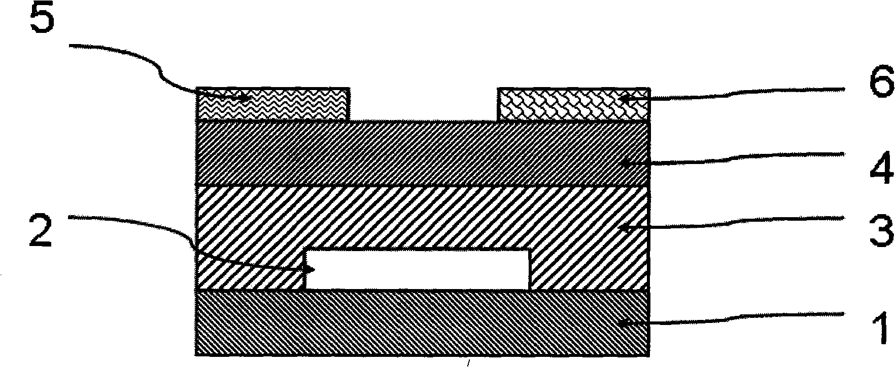
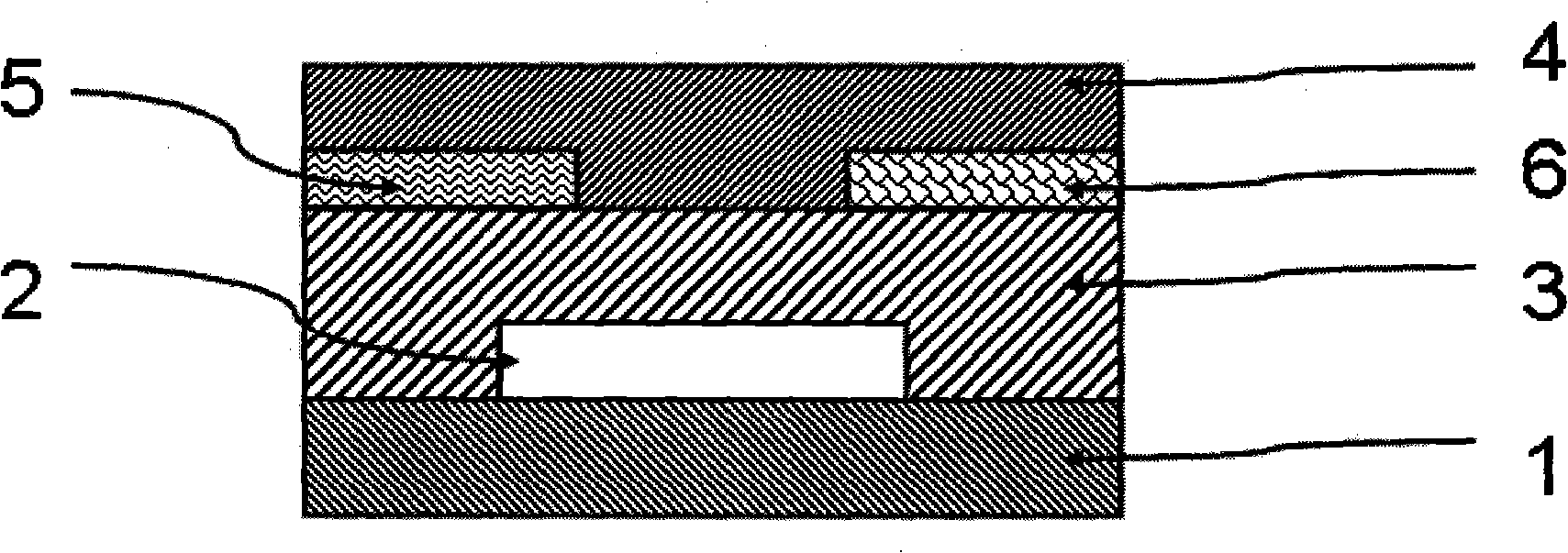
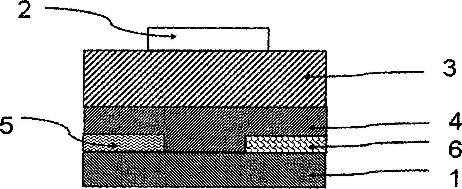
[0044] Such as figure 1 In the structure shown, substrate 1 is made of Si substrate, gate electrode 2 is made of DC magnetron sputtered ITO transparent conductive film, ultraviolet curing glue is used as gate insulating layer 3, source electrode 5 is made of Cr metal film as electrode layer, and drain electrode 6 also uses Cr metal film as the electrode layer. Conductive layer 4 is polysilicon.

[0045] The preparation method is as follows:

[0046] ① Thoroughly clean the Si substrate first, and blow dry with dry nitrogen after cleaning;

[0047] ②Gate electrodes are prepared on the surface of the Si substrate by DC magnetron sputtering;

[0048] ③Etching the ITO gate electrode pattern by photolithography;

[0049] ④ Spin-coat the UV-curable adhesive grid insulating film on the Si substrate coated with the gate electrode by spin-coating method;

[0050] ⑤ Carrying out ultraviolet curing and heating and baking the formed organic gate insulating film;

[0051] 6. Prepare a...

Embodiment 2

[0055] Such as figure 1 In the structure shown, substrate 1 is made of Si substrate, gate electrode 2 is made of DC magnetron sputtered ITO transparent conductive film, ultraviolet curing glue and silicon dioxide are used as gate insulating layer 3, and source electrode 5 is made of Cr metal film as electrode layer, and the drain electrode 6 also uses Cr metal thin film as the electrode layer. Conductive layer 4 is polysilicon.

[0056] The fabrication process of the device is similar to that of Example 1.

Embodiment 3

[0058] Such as figure 1 In the structure shown, substrate 1 is made of Si substrate, gate electrode 2 is made of DC magnetron sputtered ITO transparent conductive film, ultraviolet curing glue and silicon dioxide are used as gate insulating layer 3, and source electrode 5 is made of Cr metal film as electrode layer, and the drain electrode 6 also uses Cr metal thin film as the electrode layer. Conductive layer 4 is amorphous silicon.

[0059] The fabrication process of the device is similar to that of Example 1.


PUM


Abstract

The invention discloses a thin-film transistor, comprising a baseplate, a gate electrode, an insulating layer, a conducting layer, a drain electrode and a source electrode. The thin-film transistor is in top-contact structure, bottom-contact structure or top-grid structure; wherein the insulating layer is a combined layer which is a composite layer made of inorganic dielectric material and ultraviolet curing-requiring material or a composite layer made of a plurality of ultraviolet curing-requiring material layers. The invention is technically characterized in that the invention optimizes thin-film transistor fabrication process, improves the performance of the thin-film transistor, reduces the cost of the thin-film transistor by a large margin and reduces technique requirements and making cost for the industrialization of the thin-film transistor.

Description

technical field [0001] The invention relates to the technical field of thin film transistors. Background technique [0002] With the spread of information terminals, the demand for flat panel displays as displays for computers is increasing. In addition, with the progress of informatization, there are more opportunities to provide information that was previously provided on paper media in electronic form, and the demand for electronic documents or digital documents as thin, light, and portable display media is increasing. . [0003] Generally, in a flat-panel display device, elements such as liquid crystal, organic EL, and electrophoresis are used to form a display medium. In addition, for such display media, in order to ensure the uniformity of screen luminance and the speed of screen writing transition, etc., the technology of using active drive elements composed of thin film transistors (TFTs) as image drive elements has become mainstream. [0004] The working principl...

Claims


Application Information

Patent Timeline
Patent Type & Authority Applications(China)
IPC IPC(8): H01L29/786H01L29/51H01L21/336
Inventor 蒋亚东于军胜李璐娄双玲
Owner UNIV OF ELECTRONICS SCI & TECH OF CHINA
Why Eureka
Try Eureka