

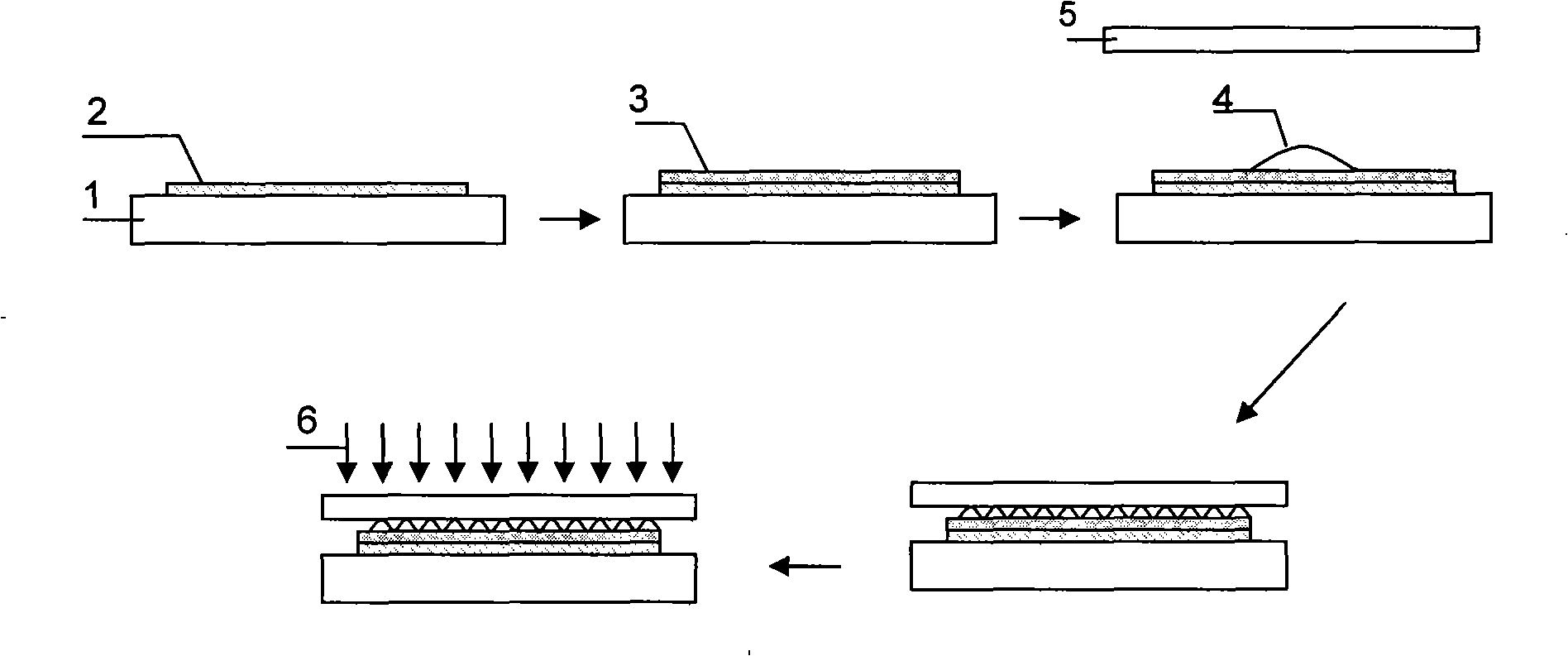
Encapsulation method for top radiation organic EL part
An encapsulation method and top emission technology, which can be applied to electric solid devices, electrical components, semiconductor devices, etc., can solve problems such as device cathode wear, and achieve the effects of low cost, simple process and short curing time.
- Summary
- Abstract
- Description
- Claims
- Application Information
AI Technical Summary
Problems solved by technology
Method used
Image

Examples
Embodiment 1
[0024] The preparation of the device is carried out in a multi-source organic molecular vapor deposition system. The detailed preparation process is as follows:
[0025] [1] The silicon substrate is repeatedly scrubbed with acetone, ethanol, and deionized water in sequence, ultrasonically, and then dried;
[0026] [2] Place the processed substrate in a multi-source organic molecular vapor deposition system (see Chinese patent: ZL03110977.2, "Crucible evaporation source for organic electroluminescence coating machine"), the same The vacuum chamber contains an organic evaporation area (8 evaporation sources) and a metal evaporation area (2 evaporation sources). The two areas and each evaporation source are isolated from each other to avoid mutual contamination. The substrate can be rotated to the organic evaporation area separately. The evaporation area or the upper part of the metal evaporation area is convenient for the growth of materials. The substrate is 25cm away from the ...
Embodiment 2
[0034] The preparation of the device is carried out in a multi-source organic molecular vapor deposition system. The detailed preparation process is as follows:
[0035] [1] The silicon substrate is repeatedly scrubbed with acetone, ethanol, and deionized water in sequence, ultrasonically, and then dried;
[0036] [2] Place the processed substrate in a multi-source organic molecular vapor deposition system. The same vacuum chamber of the system contains an organic evaporation area (8 evaporation sources) and a metal evaporation area (2 evaporation sources). The areas and the evaporation sources are isolated from each other to avoid mutual pollution. The substrate can be rotated to the upper part of the organic evaporation area or the metal evaporation area to facilitate the growth of materials. The substrate is 25cm away from the evaporation source and can rotate and revolve to ensure The uniformity of the metal film and the organic film, the materials used are placed in diffe...
Embodiment 3
[0043] The preparation of the device is carried out in a multi-source organic molecular vapor deposition system. The detailed preparation process is as follows:
[0044] [1] The silicon substrate is repeatedly scrubbed with acetone, ethanol, and deionized water in sequence, ultrasonically, and then dried;
[0045] [2] Place the processed substrate in a multi-source organic molecular vapor deposition system. The same vacuum chamber of the system contains an organic evaporation area (8 evaporation sources) and a metal evaporation area (2 evaporation sources). The areas and the evaporation sources are isolated from each other to avoid mutual pollution. The substrate can be rotated to the upper part of the organic evaporation area or the metal evaporation area to facilitate the growth of materials. The substrate is 25cm away from the evaporation source and can rotate and revolve to ensure The uniformity of the metal film and the organic film, the materials used are placed in diffe...
PUM
 Abstract
Description
Claims
Application Information