Thin-film transistor manufacturing method

A technology for thin film transistors and a manufacturing method, which is applied in semiconductor/solid-state device manufacturing, electrical components, circuits, etc., can solve the problems of complex process and high cost of thin film transistor substrates, and achieve the effect of reducing the number of lithography, reducing costs, and simplifying the process.

Inactive Publication Date: 2009-02-11
INNOCOM TECH SHENZHEN +1
View PDF0 Cites 9 Cited by
  • Summary
  • Abstract
  • Description
  • Claims
  • Application Information

AI Technical Summary

Problems solved by technology

[0021] In order to solve the problem of complex process and high cost of manufacturing thin film transistor substrates in the prior art, it is necessary to provide a method for manufacturing thin film transistor substrates with simple process and low cost

Method used


Image

  • Thin-film transistor manufacturing method
  • Thin-film transistor manufacturing method
  • Thin-film transistor manufacturing method

Examples


Embodiment Construction

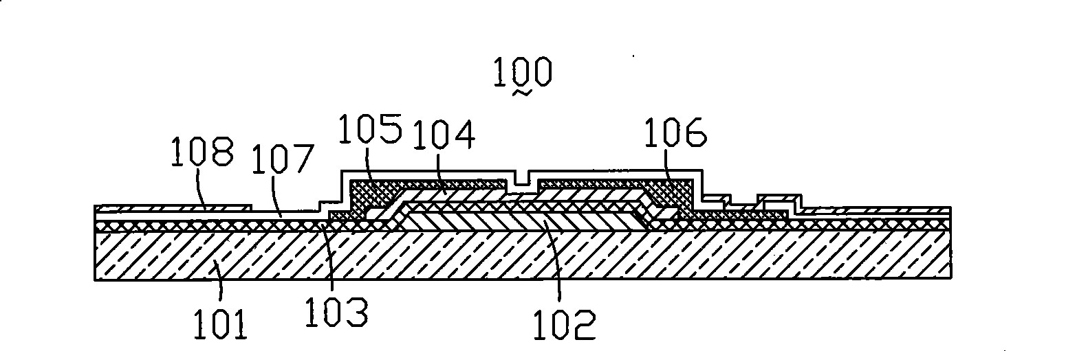
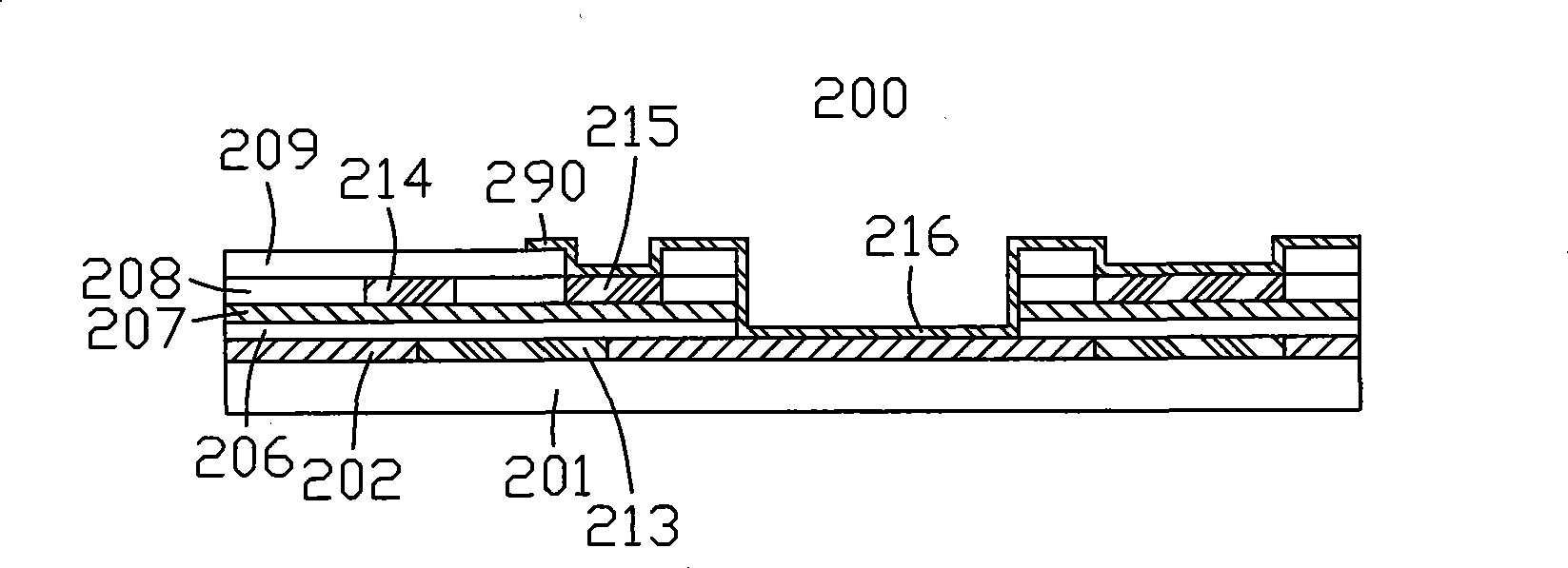
[0029] see image 3 , is a schematic structural view of the thin film transistor substrate manufactured by the manufacturing method of the thin film transistor substrate of the present invention. The TFT substrate 200 includes an insulating base 201, a gate 213 disposed on the insulating base 201, a first gate insulating layer 202, and a second gate disposed on the first gate insulating layer 202 in sequence. Pole insulating layer 206 and semiconductor layer 207, a first passivation layer 208 arranged on the semiconductor layer 207, a source electrode 214 and a drain electrode 215, a second passivation layer arranged on the semiconductor layer 207 and the source electrode 214 layer 209 and a pixel electrode 216 disposed on the drain electrode 215 and the first gate insulating layer 202 .

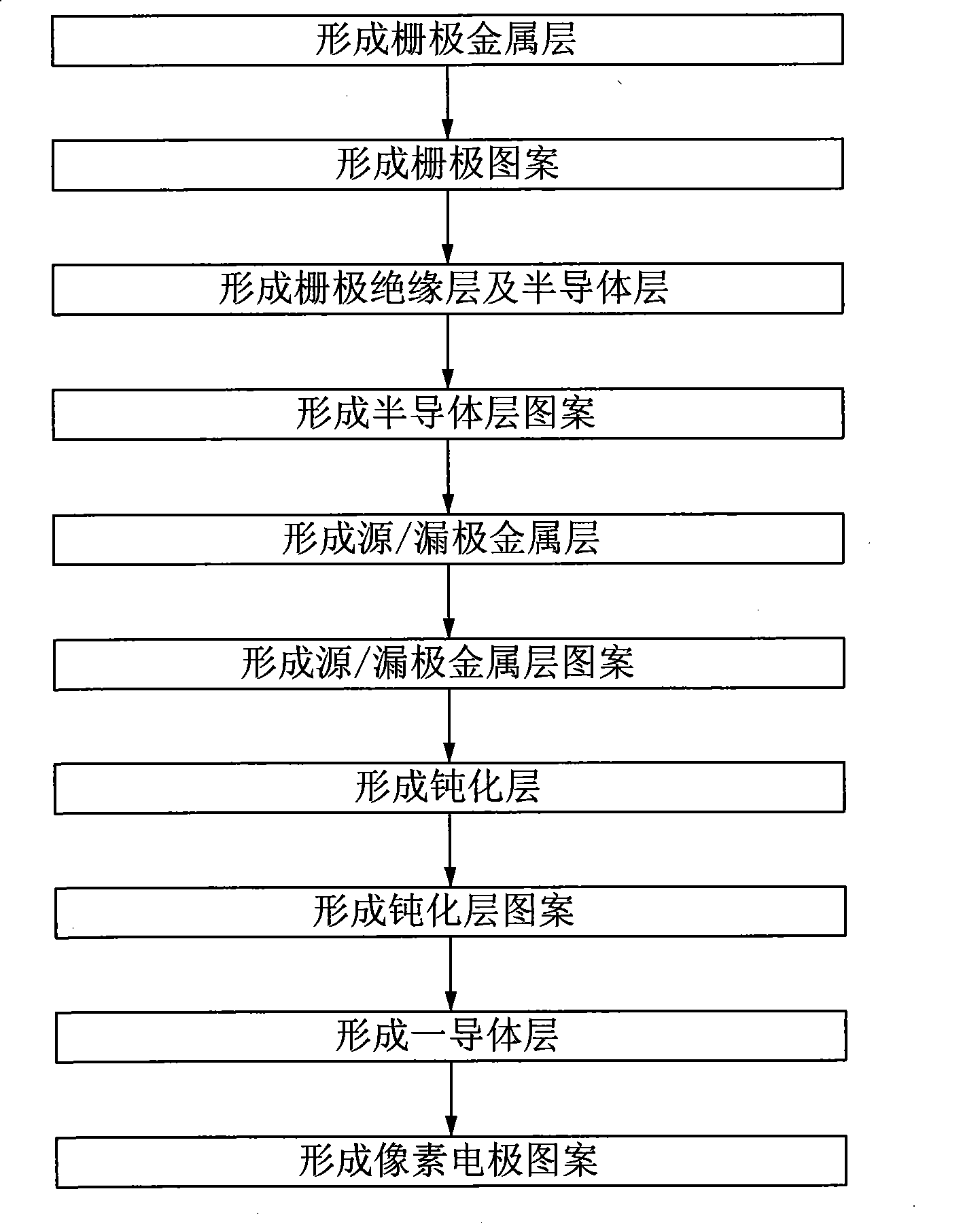
[0030] see Figure 4 , is a flow chart of a preferred embodiment of the thin film transistor substrate manufacturing method. The manufacturing method of the thin film transistor substrate...


PUM


Abstract

The invention relates to a method for manufacturing a thin-film transistor baseplate, which comprises the following steps: an insulating base is provided; a grid groove is formed on the insulating base; a grid metal layer is deposited; chemical and mechanical grinding is performed to the grid metal layer to form a grid electrode; a grid insulating layer, a semiconductor layer and a first passivation layer are deposited in sequence; a source electrode groove and a drain electrode are formed; a source / drain electrode metal layer is deposited; chemical and mechanical grinding is performed to the source / drain electrode metal layer to form a source electrode and a drain electrode; a second passivation layer is deposited; a pixel electrode groove is formed and the drain electrode is exposed; a conductor layer is deposited; and a pixel electrode is formed.

Description

technical field [0001] The invention relates to a manufacturing method of a thin film transistor substrate. Background technique [0002] At present, liquid crystal displays are gradually replacing the traditional cathode ray tube (Cathode Ray Tube, CRT) displays used in calculators. Moreover, due to the characteristics of lightness, thinness, and smallness in liquid crystal displays, they are very suitable for use in desktop computers and palmtops. Computers, personal digital assistants (Personal Digital Assistant, PDA), portable phones, televisions and a variety of office automation and audio-visual equipment. The liquid crystal panel is its main component, which generally includes a thin film transistor substrate, a color filter substrate and a liquid crystal layer sandwiched between the thin film transistor substrate and the color filter substrate. [0003] see figure 1 , is a schematic structural diagram of a thin film transistor substrate 100 in the prior art. The T...

Claims


Application Information

Patent Timeline
IPC IPC(8): H01L21/84H01L21/336
Inventor 林耀楠
Owner INNOCOM TECH SHENZHEN
Why Eureka
Try Eureka